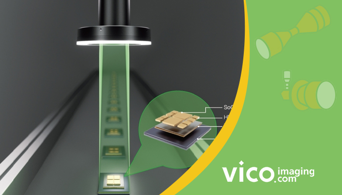
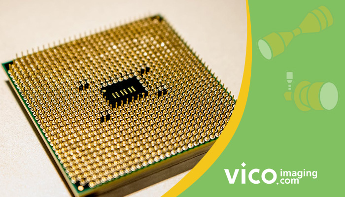
WH Series Lenses: Enhancing CoWoS Advanced Packaging Inspection in Semiconductors
Introduction: the AI Revolution and the Semiconductor I […]
WH Series Lenses: Enhancing CoWoS Advanced Packaging Inspection in Semiconductors Read More »
Introduction: the AI Revolution and the Semiconductor I […]
WH Series Lenses: Enhancing CoWoS Advanced Packaging Inspection in Semiconductors Read More »
Precision is the cornerstone of manufacturing, especial
In electronics manufacturing, you’ll often hear t
Surface Mount Technology (SMT) vs Surface Mount Devices (SMDs) – What’s the Difference? Read More »

Recently, flat-panel displays have become more popular
The flat panel display (FPD) industry has seen signific
COOLENS Industrial Lenses’ Applications in the LCM Segment of the FPD Industry Read More »
Integrated circuits, or ICs, are found in every electro
A Closer Look at IC Pin Inspection with Bi-Telecentric Lenses Read More »
Many electronic devices rely on a tiny computer chip ca
Contrary to what most people think, Automated Optical I
A Definitive Guide to Automated Optical Inspection (AOI) in 2024 Read More »
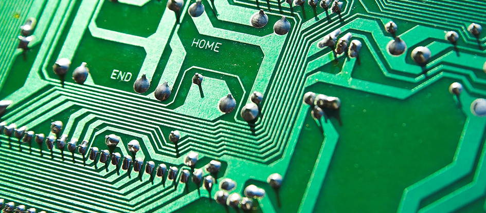
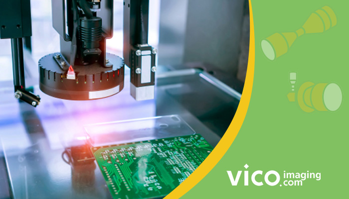
Detection object: Circuit board solder joint inspection
Circuit Board Solder Joint Inspection Read More »
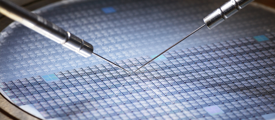
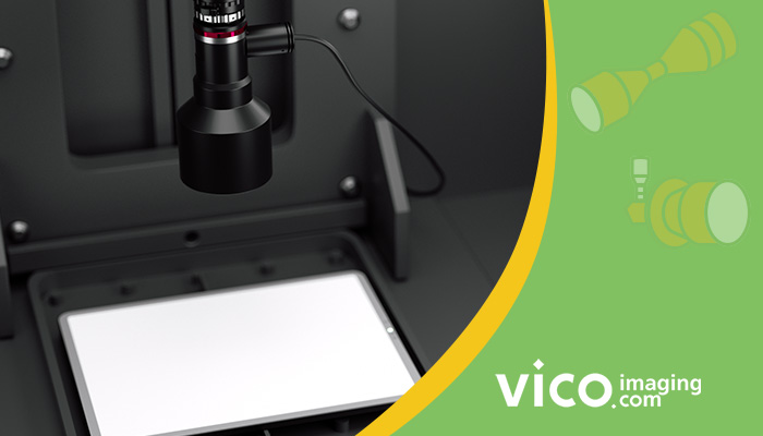
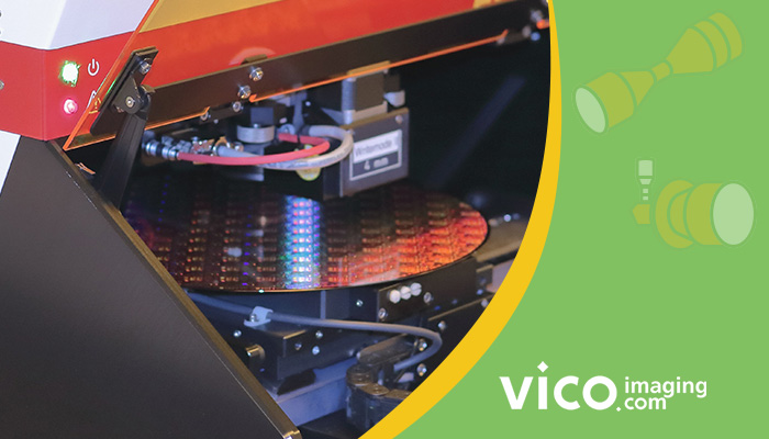
Wafer refers to the silicon wafer used in the productio
High Resolution Bi-Telecentric Lenses for Wafer Inspection in Semiconductor Read More »
Wafer refers to the silicon wafer used in the productio
High Resolution Wafer Inspection Solution Read More »
