
Many electronic devices rely on a tiny computer chip called Semiconductor. Be it computers, laptops, mobile phones, washing machines, and even cars! However, the shortage of this essential chip has recently impacted industries worldwide.
That’s because finding defects in devices and their tiny parts is getting more challenging and expensive. Manufacturers try to create small components without feature shrinkage. As a result, their designs get more complex, affecting the inspection process.
Yet, manufacturers can spot defects early by inspecting them at every production stage. An early inspection can also help companies save on costs. With step-by-step scanning, the semiconductor industry can keep yields high and costs low.
This article will explore what a Semiconductor Wafer Defect Inspection is. We will also analyze the capabilities of 24K linescan bi-telecentric lenses and their role in the wafer inspection process.
So, let’s begin!
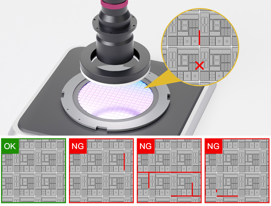
What Is Semiconductor Wafer Defect Inspection?
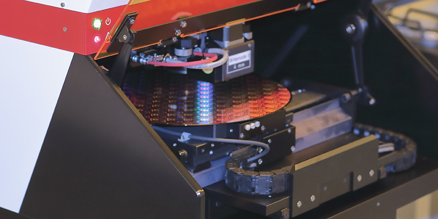
The semiconductor industry comprises layering components on a thin silicon wafer of semiconductor. This process creates tiny chips.
Each layer comes from an intricate process. The process involves adding material, forming a design, and removing waste. However, it is essential to inspect each preceding layer for flaws.
These flaws could be scratches or exposure issues. It could also be particle contamination, which we usually find before adding the next layer.
If the flaw is not found on time, it can waste resources and result in defective products. It can have a notable impact on the performance of the finished chip.
The wafer inspection process is typically performed at different crucial stages of the semiconductor manufacturing process. Manufacturers can perform it during the coating process, dicing the wafer into individual devices, packaging them, etc.
The inspection process aims to detect as many defects as possible. It does this while minimizing false warnings. It minimizes false detections using sophisticated algorithms, machine learning, and statistical methods.
For better results, it groups the defects it detects during the inspection. It then analyzes them to determine their cause and impact on the final product.
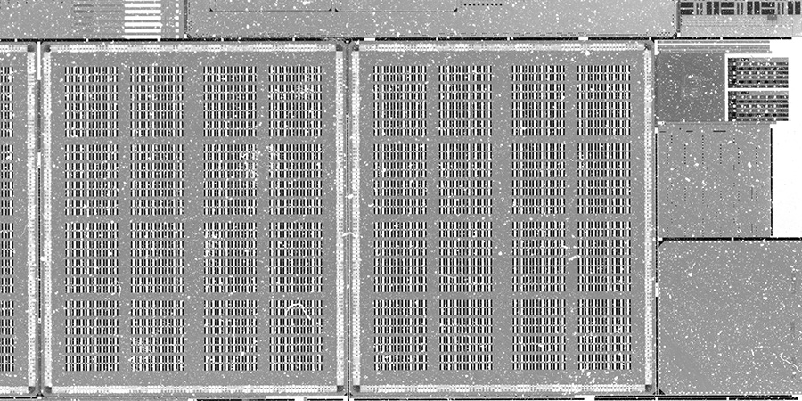
Furthermore, these flaws can occur anywhere on the wafer. They can also appear as color variations. Thus, finding them against the background of earlier layers can be challenging.
The traditional approaches to finding these flaws are not always accurate. As we all know, the manual inspection can be costly and slow. Moreover, we can perform it only on a statistical subset of wafers, making it complex.
That is why semiconductor wafer inspection is essential. Advanced tools like 24K linescan bi-telecentric lenses can help perform defect screening accurately.
What Are the Types of Defects Found in Wafer Inspection?
You can identify four main types of defects using wafer inspection equipment. These defects include:
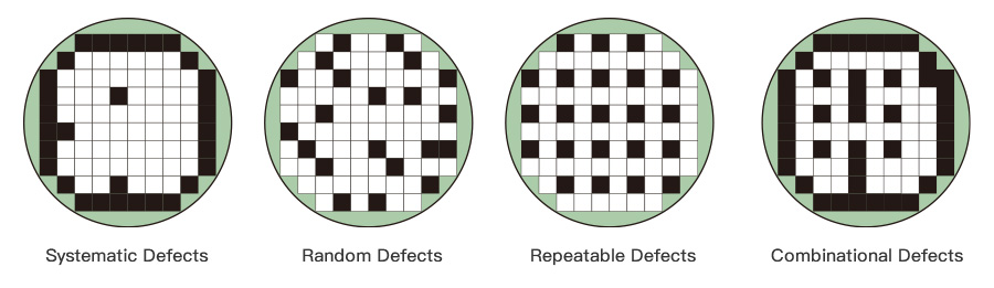
A) Systematic Defects
Systematic defects are the errors that occur during the mask and exposure process on each copy of a circuit pattern at a given area. These kinds of faults might not be detectable by conventional inspection systems.
However, systematic defects can have a significant impact on the overall performance and reliability of the final product. What’s more, they can also cause issues such as reduced yield and increased manufacturing costs.
Thus, it is crucial to identify and rectify systematic defects using advanced tools. Of course, you can do it during the wafer inspection process involving bi-telecentric lenses.
B) Random Defects
Random defects arise from particles that attach to the surface of a wafer. You cannot predict or detect them with a human eye.
A wafer inspection machine’s main job is to spot these flaws on a wafer.
After spotting the flaws, they have to pinpoint exactly where they are. Random defects can have a significant impact on performance and reliability of the final product.
C) Repeatable Defects
In wafer inspection, repeatable defects are reoccurring flaws that may be routinely discovered. You can find them in precise areas on a wafer during manufacturing.
Remember, varieties in raw materials do not cause these flaws. Instead, equipment or manufacturing processes are more frequently to blame for these flaws.
D) Combinational Defects
Combinational defects are issues arising where many features on a wafer intersect. These defects can manifest where two or more features overlap on the wafer.
Combinational defects can result from a variety of problems. These problems include variances in the materials used and the manufacturing process. Sometimes it even results from the equipment itself.
Some examples of combinational defects include misaligned features or absent or insufficient features.
What Are the Different Methods of Semiconductor Wafer Inspection?
There are different ways to carry out semiconductor wafer inspection. However, manufacturers prefer to use only a few of them. Let’s explore the effective methods to perform wafer inspection.
1) Scanning Defect Inspection
The manufacturer and the semiconductor factory carefully inspect wafers. It helps to ensure they are free of defects before production begins.
This procedure aids in locating and mapping any existing defects. It also helps while separating them from potential IC manufacturing process flaws. Only wafers with the fewest imperfections are used in manufacturing.
The defects discovered before production aids manufacturers in tracking regions with flaws. These regions can produce problems in the finished chips.
Wafers are further analyzed both before and after exposure to various processes.
After that, manufacturers use advanced optical detection systems to check wafers and masks. They scan the product for particles and other defects. The optical system can help specify their position on the wafer.
The basic theory used for identifying flaws in non-patterned wafers is straightforward. First, a laser beam scans the whole surface of a rotating wafer.
The inspection staff ensures that the beam goes onto all parts of the wafer surface. The laser light reflects off the surface of the wafer, much like it would reflect off a mirror.
When the laser beam detects a defect or particle on the wafer surface, it scatters some of the laser light. The system can notice the scattered light directly depending on how the system is set up. It can also detect scattered light as a reflected light beam’s intensity loss.
The position of the wafer helps specify the defect’s position on the wafer surface.
In this wafer inspection process, the light intensity will be recorded electronically. It does this using a PMT or CCD.
It also records the map of scattered light generated over the wafer surface. This map provides data on the size and location of the defects. It also includes information on the condition of the wafer surface, like particle contamination.
Remember, this method requires high accuracy. It needs repeatable linear and rotary control of the wafer stage. Moreover, it also needs highly advanced optical components.
The surface roughness can have a significant impact when the size of defects becomes smaller. That’s because it reduces the signal-to-noise ratio of the scattered light. Thus, inspecting wafers for defects smaller than 100 nm is challenging.
The signal-to-noise ratio is a crucial factor. It helps determine an inspection system’s ability to detect minor defects. Additionally, surface chemical contamination, such as humidity, can decrease the signal-to-noise ratio.
Inspection tools for detecting sub-100 nm defects use advanced optical filtering polarization analysis. They also use specialized signal processing algorithms. It helps to detect defects even in the presence of surface haze.
2) Topography Inspection
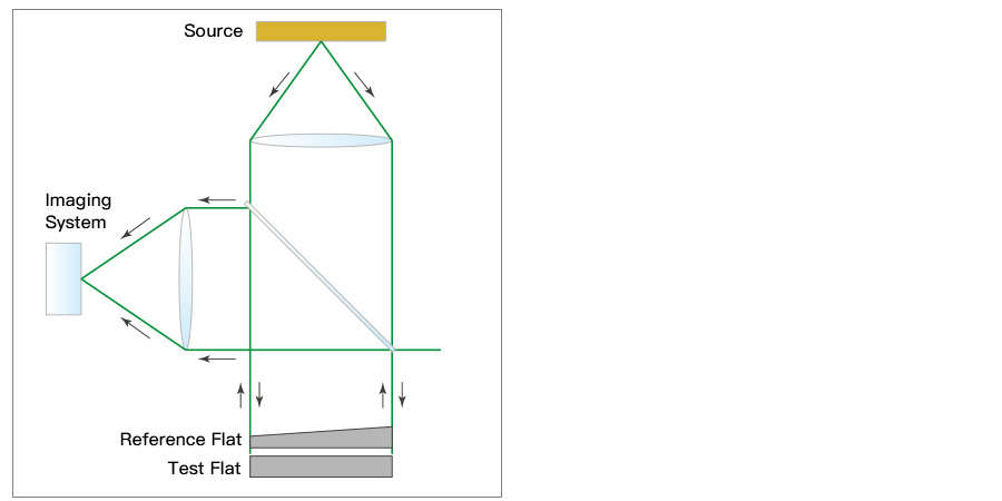
Manufacturers measure a bare wafer’s shape for many reasons. For instance, the wafer may bend or develop dents due to the machinery used to hold it during processing. At small sizes, these deformations can affect pattern production on the wafer.
So, how can you identify such minor dents or bends? The interferometer is an accurate instrument to carry out this task. You can use this tool to measure variations in wafer shape before processing.
These instruments share a fundamental design with another device. It contrasts the wafer with an extremely flat and smooth reference surface.
After that, it creates a light reflection from the reference surface. It contrasts with the light reflecting from the wafer.
The shape of the wafer is then mapped out with extremely high precision. This precision is down to a few nanometers. It uses advanced software after examining the two light reflections.
You may need an advanced imaging system to meet the required level of precision. You will also need huge optics and intense lighting to attain this level of accuracy.
3) E-beam Wafer Inspection
Electron beam (EB) imaging is another way to inspect defects. This technique is beneficial for finding faults of extremely small sizes. It is useful where the optical imaging system turns less efficient. Compared to basic optical inspection methods, the EB examination offers a higher level of accuracy.
Yet, because EB imaging is so slow, its application is primarily confined to R & D purposes and testing new technologies. Numerous EB instruments are being created each year to help inspect smaller defects. Also, new EB tools are being created that can detect flaws as small as 10 nanometers.
4) Reticle Inspection
Reticles are unique masks that project patterns onto wafers during the manufacturing process. These masks have fine features, typically 4 to 5 times larger than the desired pattern on the wafer.
You can use them with optical systems that can transmit light through the mask. They then shrink the pattern onto the wafer.
The reticle inspection is more critical than inspecting either patterned or non-patterned wafers. It is because a single defect on a reticle can ruin many devices. It happens since defects will repeat on every wafer processed with that reticle.
Reticle inspection systems work on similar principles as wafer inspection tools. However, they use transmitted light instead of reflected light.
These tools have high-resolution imaging optics. Besides, they use either visible or UV light. It depends on the feature size and defect tolerance.
Inspections happen during reticle production and throughout reticle usage. These tools use special image analysis software. They also use motion control systems like wafer inspection tools.
Conventional optics in reticle inspection systems extend to 90 nm feature sizes. The extension is by using UV illumination.
Reticle inspection at smaller feature sizes is also possible. It uses an electron beam (EB) since it can tolerate lower throughputs.
Reticle inspection tools employed in sub-100 nm applications use DUV illumination. It means using a single wavelength at 266 nm or 193 nm.
Why Are Bi-Telecentric Lenses Suitable for Wafer Inspection?
We use different electronic devices in our daily lives. These devices include mobile phones, computers, TVs, etc.
They all rely on chips to perform storage and data processing functions. The core of each chip consists of a wafer, which comes from wafers of different specifications.
Wafers themselves can have problems with yield. There may be various defects found on the wafer surface. Manufacturers use optical inspection equipment to determine, classify and mark these defects.
They do this to prevent the use of defective wafers in packaging. The overall inspection process happens on the wafer surface and assists in wafer sorting.
Optical inspection equipment includes devices like optical lenses and industrial scanning cameras.
The inspection instrument also includes light sources and vision processing systems. It can replace the conventional manual visual inspection process. That’s because it helps to achieve precise identification of scanned items. It also enhances inspection efficiency.
Bi-telecentric lenses are suitable for wafer inspection. It is because they provide several key advantages over other types of lenses.
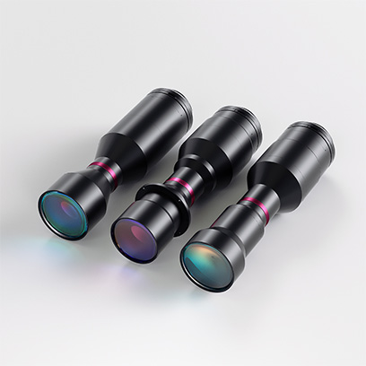
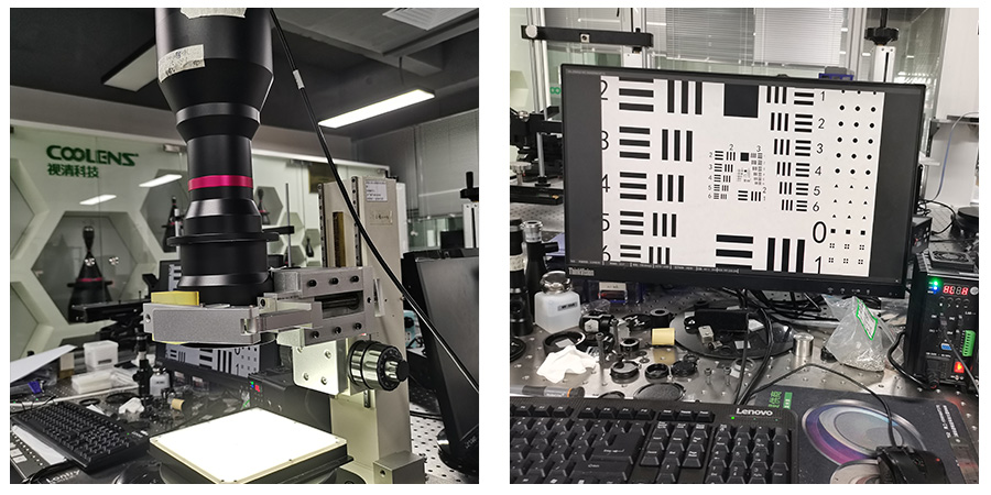
Why Do We Recommend 24K Linescan Bi-telecentric Lenses?
Bi-telecentric lenses combine the benefits of object space and image space telecentric lenses. Thus, it’s no wonder why these lenses have become a vital part of wafer inspection process in the semiconductor industry!
Telecentric lenses, especially object space, are common in industrial image processing. Likewise, image-space telecentric lenses are not practicable in industrial image processing and machine vision.
That’s why we recommend using bi-telecentric lenses that are telecentric on both sides. The 24K linescan bi-telecentric lenses are highly useful in wafer inspection.
1) 2.0X Constant Magnification
First, bi-telecentric lenses maintain a constant magnification across the entire field of view. It means the size of features on the wafer will appear the same size regardless of their position on the wafer.
It is essential for ensuring accurate and consistent measurements of the wafer’s surface. You can learn about the magnification of the lens to better understand this point.
Our DTCA series of bi-telecentric lenses features 2x magnification, giving you a more detailed image of an object.
2) Excellent Resolution
As you know, bi-telecentric lenses have a considerable depth of field. It means they can focus on objects at different distances from the lens.
When doing this, they do not lose image sharpness. It is beneficial for wafer inspection. It allows the lens to capture the wafer’s surface for any defects or particles. These defects may be present on the wafer surface.
3) Large Aperture F/4.8
Bi-telecentric lenses have a large aperture (F/4.8). They can capture more light and produce images with a higher level of detail. It is critical for detecting minor defects or particles on the surface of the wafer.
4) Wide Image Circle
Finally, bi-telecentric lenses are highly stable. Besides, they have a wide image circle, which can easily suits to 3.5 μm linescan cameras and 88 mm sensors. They maintain their imaging performance over a long period. It is vital for a consistent and reliable inspection process.
FAQs:
1) What Is a Patterned Wafer Inspection System?
A patterned wafer inspection system is a specialized tool for inspecting semiconductor wafers. These wafers have patterns with features such as transistors, interconnects, and other components.
The technique checks for flaws and irregularities in the wafer’s pattern. It helps find defects that can affect the reliability and performance of the finished electronic devices.
In a patterned wafer inspection system, defect inspection is performed by checking and comparing the pattern images of adjoining chips and getting the difference.
Remember, manufacturers perform patterned wafer inspection on processed wafers.
2) What Is a Non-Patterned Wafer Inspection System?
A non-patterned wafer inspection system is a tool used to detect defects during the early production stages of the semiconductor.
It inspects and analyzes a wafer’s surface with no patterns or structures on it. Thus, defect detection occurs without comparing images.
3) Why Use Linescan Lenses?
Linescan lenses have numerous uses in industrial image processing and machine vision applications. They capture images of objects that are moving past a stationary camera.
These lenses provide a narrow, elongated field of view. It allows them to simultaneously capture a single, highly detailed line of an image.
Remember, linescan lenses are useful for applications that require high-resolution images during the inspection. Besides, some inspection systems require fast image acquisition with low distortion. Wafer inspection is one such application.
They are typically used in conjunction with a line scan camera. The camera captures the image line-by-line as the object moves past the lens.
Final Thoughts!
Nowadays, semiconductors are becoming smaller with more complicated designs. Thus, finding defects in wafers is becoming very expensive.
However, manufacturers can still identify minor defects quickly. They can cut costs by performing the inspection at every stage of manufacturing.
Bi-telecentric lenses have revolutionized the way of inspecting wafers. They offer a unique inspection solution that is both correct and reliable.
A key instrument in the wafer inspection procedure is 24K linescan bi-telecentric lenses. These lenses can help identify and locate many defects in less time. These defects can be combinational, random, repeatable, and systematic flaws.
Of course, finding these defects at the right time is a challenging task. One minor flaw can ruin the entire production cycle.
So, go ahead and get the right instrument for your inspection process. At VicoImaging, you can find numerous types of lenses, including telecentric, bi-telecentric, etc. We also offer different useful optical accessories to help support your inspection set-up. Contact VicoImaging today!
