
Introduction: the AI Revolution and the Semiconductor Industry
The AI boom has reshaped the semiconductor industry, positioning chip-making companies at the forefront of technological innovation.
With the increasing demand for AI chips, companies like TSMC are urgently seeking equipment suppliers for CoWoS (Chip on Wafer on Substrate) devices. CoWoS, a high-density advanced packaging technology developed by TSMC, has become a crucial factor in AI chip production. Addressing the current CoWoS packaging capacity shortfall is essential to meet the growing AI-fueled demand.
In this context, the VICO Imaging Lenses vision inspection solution plays a significant role in the CoWoS process. It’s pivotal for quality control, ensuring the integrity and correct placement of components during the packaging process, which is vital for TSMC’s efficient CoWoS encapsulation.
Understanding Wafer and Chip Packaging Technology
– Explanation of wafer packaging and its necessity for protecting fragile chips and enabling connections with external circuits.
– Description of traditional packaging and its limitations.
– Discussion of the evolution of packaging technology, from traditional methods to CoWoS encapsulation.
The Challenge of CoWoS Packaging Capacity
Currently, the limited capacity for CoWoS packaging is emerging as a significant bottleneck in the production chain for AI chip orders. In response, TSMC has ramped up its equipment orders by 30% to tackle this challenge head-on. This strategic move is not just about meeting current demands but also about future-proofing TSMC’s manufacturing capabilities in the face of an AI-driven market.
The Role of VICO Imaging Lenses in CoWoS
Enter VICO Imaging Lenses, a game-changer in the realm of semiconductor inspection. These lenses are specifically engineered for the CoWoS packaging process, playing a crucial role in ensuring the quality and accuracy of chip assembly. Their vision inspection solution is a key component in the mid-inspection phase of the CoWoS process, focusing on detecting damages, misalignments, and ensuring the correct placement of chip components.
Understanding Wafer and Chip Packaging Technology
The journey of a wafer from a delicate, fragile state to a robust, functional chip is a marvel of modern engineering. This transformation is made possible through advanced packaging technology, which not only protects the chip but also enables efficient connections with external circuits. Let’s delve into the details of this critical process.
Traditional Packaging Techniques
Traditionally, chip packaging involved a series of steps starting from the back-end grinding of the wafer to cutting it into individual dies. The dies, each representing a potential chip, are then meticulously extracted and prepared for assembly. This conventional approach, while foundational, had its limitations, particularly in terms of size and connectivity.
The Evolution of Chip Packaging
Over the years, packaging technology has evolved dramatically, driven by the twin goals of protecting the chip and enhancing connectivity. This evolution can be categorized into four distinct stages, each marked by innovative approaches and techniques:
Die Bonding Stage
This stage represents the basic traditional packaging process, focusing on the physical assembly of the chip onto a substrate.
Flip-Chip Packaging
A significant leap from traditional methods, flip-chip packaging involves direct attachment of the chip onto the substrate, offering improved connectivity and reduced size.
Wafer-Level Packaging
Here, the packaging process is applied to the entire wafer before individual chips are cut, streamlining the process and reducing costs.
2.5D and 3D Packaging Techniques
Representing the cutting edge of packaging technology, these methods involve complex layering and integration of chips, significantly enhancing performance and reducing space requirements.
CoWoS: A New Frontier in Chip Packaging
CoWoS stands out as a revolutionary approach in the semiconductor packaging landscape. It represents a 2.5D integration technique, marrying logic computing and HBM chips through a silicon interposer. This approach not only maximizes the efficiency of the chips but also addresses the critical need for high-density integration in modern computing applications.
Diving Deep into CoWoS Packaging
In a typical CoWoS package, the central logic IC is surrounded by multiple GPU units and HBM (High Bandwidth Memory) components. This configuration is crucial for high-performance applications, especially in the realms of AI and high-speed computing. HBM, in particular, plays a vital role, offering significantly higher memory bandwidth compared to traditional memory technologies like DDR4.
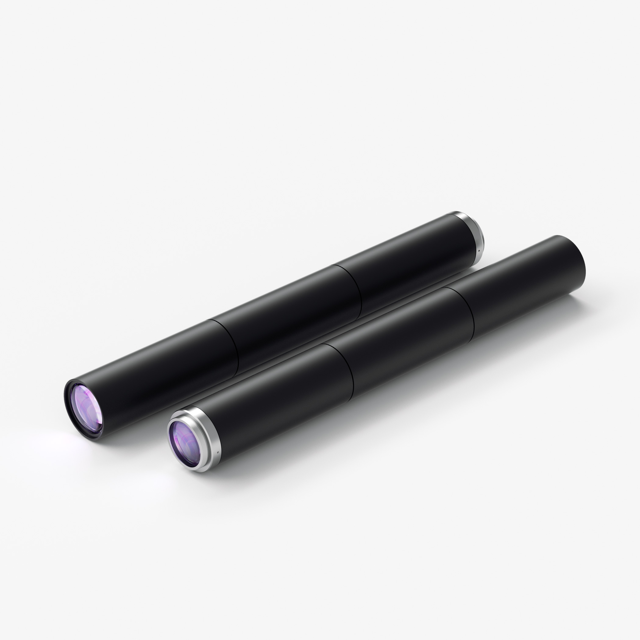
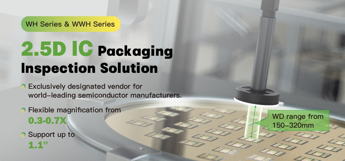
VICO Imaging WH Series Lenses: Precision Inspection Tools
In the intricate world of CoWoS packaging, precision is key. This is where the WH Series Lenses from VICO Imaging come into play. These lenses are designed to inspect the minutely detailed structures within a CoWoS package, ensuring that every component, be it the CPU, GPU, or HBM, is perfectly aligned and free from any defects.
Unique Features of WH Series Lenses
Magnification Range
The lenses offer a flexible magnification range of 0.4x to 0.5x, ideal for inspecting the intricate details of CoWoS packages.
Long Working Distance
The lenses provide a long working distance, a crucial feature for accommodating different mechanical structures in semiconductor inspection.
High Depth of Field
With their high depth of field, these lenses can simultaneously focus on multiple layers of a chip, ensuring comprehensive inspection of all components.
The Impact of VICO Imaging Lenses in CoWoS Inspection
The WH Series Lenses have become an indispensable tool in the CoWoS inspection process. By offering a precise view of each component’s placement and detecting even the slightest misalignments or damages, these lenses significantly contribute to the overall quality and reliability of the semiconductor products.
The Future of Semiconductor Inspection with VICO Imaging
Looking ahead, the role of advanced lens technology like the WH Series in semiconductor inspection is only set to grow. As chips become more complex and the demands for precision and efficiency increase, tools like VICO Imaging Lenses will continue to play a critical role in shaping the future of semiconductor manufacturing.
Conclusion
The journey of semiconductor manufacturing is one of relentless pursuit of perfection, where each component, no matter how small, plays a crucial role in the functionality of the final product. The WH Series Lenses from VICO Imaging stand as a testament to this pursuit, representing the pinnacle of precision and innovation in semiconductor inspection.
As we continue to push the boundaries of what is possible in chip technology, the importance of advanced inspection tools like these lenses can not be overstated. They not only ensure the quality of today’s semiconductors but also pave the way for the technological breakthroughs of tomorrow.
