
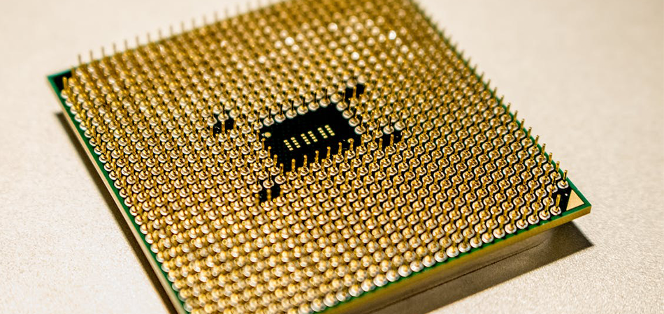
Integrated circuits, or ICs, are found in every electronic device. They are made of many discrete parts that are all integrated into a small silicon chip.
As technology advances, the complexity of integrated circuit components increases – requiring careful pin inspection to ensure they fulfill the highest standards of quality control.
A PCB manufacturer must use datasheets or other sources to complete the circuit connections to get an idea of the pins. However, the circuit will ultimately fail if the pins are misconnected.
That’s why optical inspection has recently become essential to assure quality throughout different manufacturing operations. The manufacturing of IC sockets is the best example to describe this kind of process.
If you want to ensure that each pin on an IC works appropriately, you must inspect it visually. Moreover, you can also use advanced technologies like AOI to perform accurate pin inspections.
This post will explore what pin inspection means for integrated circuits. Moreover, we will also discuss how you can use modern tools like bi-telecentric lenses to perform pin inspections.
What Exactly Is IC Pin Inspection?
Pin inspection is a method used by manufacturers to check the electrical connections between two or more points on an IC package for any flaws or irregularities.
It involves inspecting pins with specialized tools such as microscopes or lenses and ensuring their physical characteristics match those specified in the relevant datasheet.
It helps identify signs of wear or damage that might go unnoticed during assembly, potentially leading to substandard IC performance or even IC failure.
There are several reasons why ICs fail. Manufacturing flaws, physical damage, electrostatic discharge (ESD), and extreme operating temperatures are the most common causes of IC failure. And most importantly, there are pins that can be problematic too.
Pin inspection is a vital step that confirms each IC component can work at its best. It helps locate potential manufacturing flaws or defects before production begins, ensuring that only high-quality products reach customers.
With careful pin inspections, manufacturers can stay assured that their ICs have been tested thoroughly against industry standards. Besides, regular pin inspections can help manufacturers identify potential issues before they become costly or time-consuming.
In addition to visual inspection, companies also use the automated optical inspection (AOI) technique. It uses industrial cameras to capture images of the object to be inspected. This method is commonly used in the electronics industry to ensure that the positions of the soldered pins are within the specifications.
The inspection results are then obtained through image processing. In short, modern technology can reduce human error and save pin inspection time.
Some Common Methods of IC Pin Inspection
Several methods are used for pin inspection depending on the type and complexity of the IC being inspected.
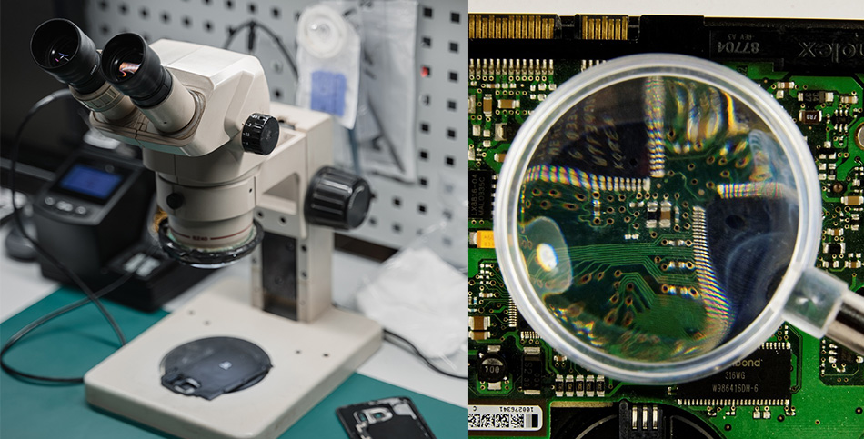
For simple IC chips, manual visual inspections can be performed by trained workers using traditional magnifying glasses or microscopes.
Besides, the AOI system works best for both simple and complex ICs. This method can quickly check pins with higher accuracy than humans.
X-Ray Inspection

X-ray inspection is the most advanced method of inspection for BGAs. It works by projecting X-ray energy onto the board through an X-ray tube.
In this method, X-rays pass through the board and get trapped in dense areas like solder joints. Then, the rays are collected at a detector, where they are converted into visible light, and an image is produced.
The viewer can see solder patterns because the solder joints in this image are darker than their surroundings.
This method is ideal for identifying solder bridges, inspecting pins, detecting excess solder, and other similar defects. The resulting images help you observe solder patterns and shape variations.
X-ray inspection methods, like endoscopes, can be used for many other applications, including through-hole inspection, surface-mount defect analysis, unleaded solder inspection, etc.
Optical Inspection
The use of optics technology to examine pins is referred to as optical inspection. In the past, this method used to rely on the naked eye or microscopes, delivering ineffective results with errors.
But now, using modern tools like bi-telecentric lenses has been proved quite crucial for this inspection method. The ability of the lenses to inspect small objects in small spaces makes them ideal for pin inspections.
The technology uses a camera with a high-magnification lens and a connected monitor to get close-up images. This technology is frequently used with visualization software to achieve better image capturing and measurement results.
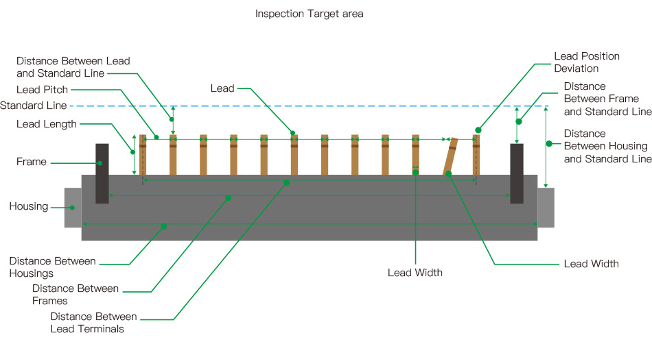
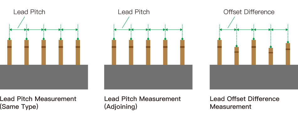
Technicians can examine the outer row of pins using visual inspection. If adequate lighting is provided, they can also check some interior rows.
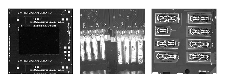
An IC can have various defects on different parts, like the solder joint’s shape, surface texture, bent pins, and appearance. However, these defects can be identified and evaluated using this optical technique.
Optical inspection is the best method since it can identify opens, shorts, damages, debris, and cold solder. Through careful observation, one can identify any signs of corrosion, wear, or tears on the pins quickly and easily. This technique also detects abnormalities like discoloration or misalignment.
Electrical Testing
Another method of inspection that examines the board’s electrical properties is electrical testing. It differs from mechanical testing, which puts the board through shock and shear tests to see how well the solder joints hold up under stress.
This method passes a current through the board to evaluate the board’s electrical stability. The purpose of this kind of test is to know whether there are any electrical issues like shorts or opens.
Yet, as we mentioned, electrical tests cannot be used to find the location of a defect, especially if it is related to pins. Even though electrical testing is an integral part of a pin inspection, it is not as reliable as optical inspection.
All these approaches have advantages and drawbacks, but they all offer an effective way to identify obvious and hidden defects during pin inspection.
However, we recommend using the optical inspection method for better results. It uses advanced tools like bi-telecentric lenses, which get your pin inspection process much closer to accuracy.
What Is Needed for IC Chip Defect Visual Inspection?
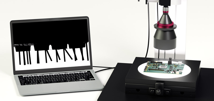
A proper pin inspection of an IC requires patience and precision. But more than that, it also requires an advanced setup.
The machine vision setup for IC pin inspection consists of a computer, an industrial camera with a bi-telecentric lens, an LED ring light, and a diffuser.
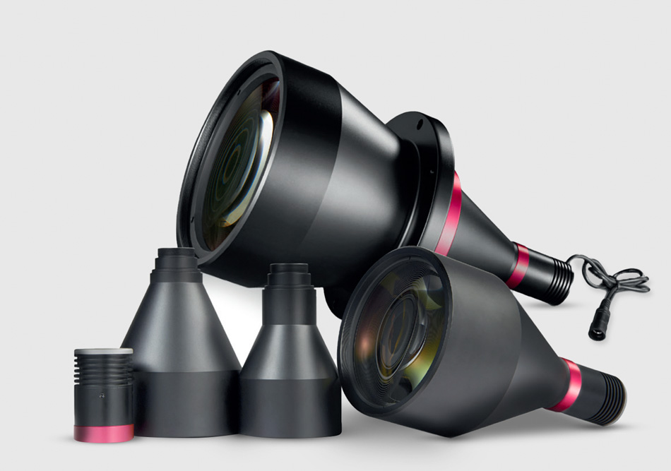
Lens
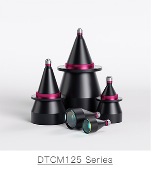

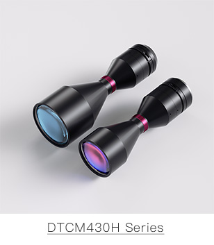
The world of electronics has been constantly evolving, and staying ahead of the competitors means being aware of the latest tools available. Bi-telecentric lenses are one such tool that provides many advantages when performing IC pin inspection. Improved image resolution is one of those advantages.
VicoImaging studies and designs the best industrial lenses to meet industry standards. Our lenses can fulfill the requirements for precise imaging and defect identification.
We have designed different models of bi-telecentric lenses specifically for IC pin inspection applications. Thus, they are extremely user-friendly and require minimal setup time compared to other magnifying devices.
Camera
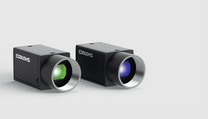
The machine vision setup also includes a high-speed industrial camera that meets the following requirements, including:
- Stable transmission
- High image quality
- High-speed photo recognition
- Automatic and efficient detection
Light Source
 Elecentric Illuminators
Light source plays a crucial role in improving the reliability and efficiency of an optical inspection system. LEDs have the edge in this context since they provide stable light without generating heat.
You can use an external coaxial light source to achieve excellent picture uniformity in a machine vision setup.
System for Image Analysis
The final component of IC pin inspection with bi-telecentric lenses involves using advanced software to analyze image data obtained by the lens itself.
Through advanced algorithms, it is possible to detect any irregularities within pins or traces on ICs before they lead to product failure.
So, having outlined the setup for IC pin inspection with bi-telecentric lenses, let’s now focus on the actual inspection process.
How Does Pin Inspection of IC Chip Work?
Once the setup required for optical inspection is ready, you can proceed to the actual pin inspection operation.
You can use an LED ring as a primary light source. Then, position the diffuser in front of the light source to produce back-diffused light. It will help distribute light evenly across the entire image being produced.
The camera attached with a suitable bi-telecentric lens will capture the image. After that, it will be sent to a PC for further image processing.
Lastly, the software will generate reports detailing both correct and defective pins based on specified parameters.
Tips for Pin Inspection of ICs
During production, IC manufacturers employ various inspection techniques to guarantee the ICs’ production quality. Every manufacturer must follow best practices to ensure a successful pin inspection.
Know the Basics
Before inspecting, you must have a basic understanding of ICs. It includes their function, main electrical parameters, the role of each pin, standard voltage, etc.
Use the Right Equipment
Tools have always been an essential component of every inspection process. However, selecting the appropriate tools for inspection can be challenging.
For optical inspection, you must use high-quality lenses manufactured by a reputed brand, like VicoImaging.
Check the Pins Thoroughly
The pins on an integrated circuit (IC) chip connect the tiny components. Thus, make sure you test each pin. Of course, it may not be possible during the manual inspection.
That’s why you must use modern technology like AOI to simplify the inspection process further.
FAQs:
Is IC Pin Inspection a Tedious Task?
Inspecting IC pins requires careful assessment and attention, and it’s not always easy. Every time you think you’ve discovered an issue, another one pops up in its place. So the manual inspection process is much more time-consuming and tiresome.
Don’t worry! You can save time by using specialized tools and instruments.
Should IC Pin Inspection Be Performed?
Remember, ICs consist of tiny components responsible for many vital functions. However, we assume they will continue to work without supervision, inspection, or quality control.
Pin inspection is an essential process that ensures each IC component works at its best. So, you cannot exclude this process.
Which Lens Is Suitable for IC Pin Inspection?
Bi-telecentric lenses are the best choice for IC pin inspection since they offer increased magnification. These specialized lenses offer numerous advantages over other traditional lenses used for inspection.
Final Thoughts!
Pin inspection of ICs is an essential part of the manufacturing process. With appropriate techniques and best practices, pin inspection can help companies create reliable products that meet their customers’ needs.
As you can see, bi-telecentric lenses provide an innovative approach in the field of pin inspection.
At VicoImaging, you will find different models of bi-telecentric lenses. We understand the features a specific lens should have for successful pin inspection. Order your lenses now!
