
The electronics manufacturing business is characterized by a high level of professionalism. Individuals who have knowledge in this domain tend to use fundamental abbreviations to express their requirements, including but not limited to PCB (printed circuit board), PCBA (PCB assembly), and Through Hole Technology (THT), among others.
In addition, it is worth noting that the acronyms SMT (Surface Mount Technology) and SMD (Surface Mount Device) frequently appear in relevant discourse. However, what do they entail? Which is better, SMD or SMT, and why?
Well, there is a common confusion between these two abbreviated terms within the realm of electronics manufacturing. The distinction between Surface Mount Technologies (SMTs) and Surface Mount Devices (SMDs) extends beyond a mere terminology discrepancy, including many factors. Primarily, one may be characterized as a procedural operation while the other can be classified as a device.
Here, we’ll highlight the distinctions between the two abbreviations. That’s not all, however; you’ll also learn every detail of each phrase, beginning with its meaning.
Surface Mount Technology (SMT): What Is It?
Surface mount technology means mounting and soldering parts onto a circuit board. This technology gained widespread use in the electronics industry in the 1980s. Costs decreased, and efficiency increased as methods and technologies were fine-tuned. SMT has helped electronic companies and their customers save money by reducing the number of devices used in their products while also improving performance, adding features, and decreasing error rates.
Smaller parts, a more streamlined production process, fewer mistakes, and more efficiency contribute to significantly reduced manufacturing costs. Industries that depend on flawless performance have taken notice because of these advantages.
There has been a rise in the use of SMT in several industries, including consumer electronics, transportation, healthcare, and communications. These sectors could not have grown and expanded without SMT, eliminating the need for a less effective and more prone to mistakes procedure.
Basic Concept
Surface mount technology, or SMT, is a technique for assembling printed circuit boards. It involves directly mounting electrical and electronic components onto the PCBs’ surfaces.
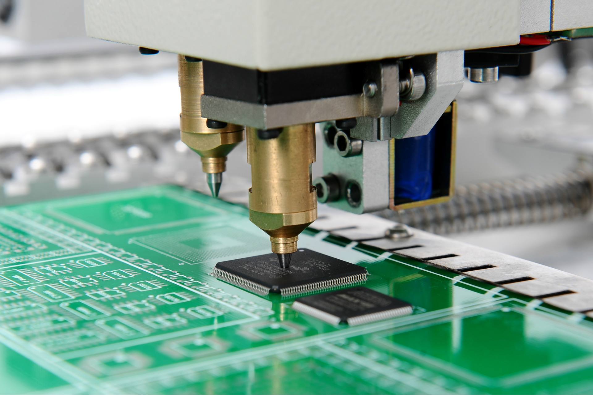
This method involves applying solder paste to the surface of the boards to achieve accurate alignment of a stencil. The stencil guides the pick-and-place machine as it places explicitly the components on the boards. Afterward, the boards are heated in infrared ovens to soften the solder paste and form the solder connections.
Characteristics of SMT
– SMT makes it easier to create compact electronics or gadgets
– This technology helps minimize parasitic capacitance as well as inductance
– It cuts down on the number of needed PCBA parts
– Modern, automated machinery allows for consistent, high-output
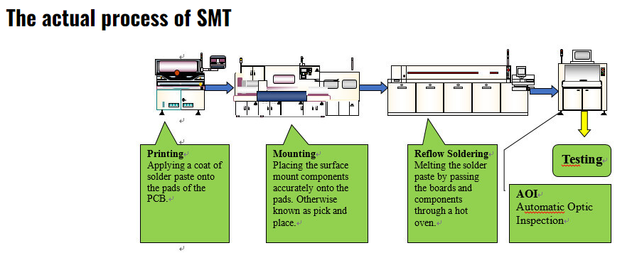
SMT Assembly Process
Printing
Before printing, the SMT instrument places the stencil over the patched area of the PCB board. Squeegeeing the stencil outward deposits solder paste onto the appropriate solder joints via the openings.
Mounting
The solder paste serves as a temporary glue while a pick-and-place machine precisely positions the SMD components.
Reflow Soldering
Reflow soldering is the process of melting and solidifying solder paste, which is currently in a semi-liquid condition. It helps create a strong solder connection. The SMT method often employs reflow soldering when working with small-pin parts like ball grid arrays. It allows for exact temperature control and consistent heat distribution, leading to excellent solder joints.
Testing and Inspection
After the SMT process flow finishes, the manufacturer performs several inspection procedures to test for component position, solder bridges, short circuits, etc. These checks use various methods, including manual inspection, AOI inspection, and others.
To install every part securely, SMT assemblers use just the proper quantity of solder paste. Component mounting on the PCB can also be automated by instructing a machine to do it. It not only speeds up the manufacturing and delivery times but also guarantees correctness.
Surface Mount Device (SMD): What Is It?
A surface-mounted device (SMD) is nothing but an electrical part connected to a circuit board. The very effective and accurate SMT is what inspired the development of SMDs.
Basic Concept
SMDs, or surface-mounted devices, are electronic parts that are connected to circuit boards during assembly. Their compact size directly results from the market’s need for more efficient and affordable technological devices.
As technology became smaller and more complex in the latter half of the 20th century and towards the 21st century, through-hole methods became obsolete. Traditional parts were not only bulkier but also installed more slowly. SMDs employ pins rather than wire leads to connect to the board’s pads. Because no holes need to be drilled, the whole board may be put to good use rather than wasted.
SMD Characteristics
– Leads are either absent or very short on an SMD.
– It minimizes through-holes on PCBs, thereby preventing manufacturing mistakes.
– Improved efficiency despite reduced size
– It allows the solder joints and the SMD body to be on the same side.
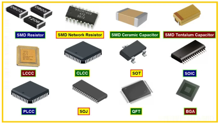
SMD Components
Just 20 years after their introduction, SMD components have grown to dominate the industry. Surface mount devices are quite popular these days due to their growing use. You will find a great diversity in SMD components. Below you will find a list of all important SMD components.
Resistor:
The SMD resistor is often surface-mounted using SMT technology. However, its installation requires extra care. They usually have electrodes connected on each end. These are available in two types, including thick and thin film. When talking about the surface mounts, you will come across the term R-packs. These are resistor networks that help save placement time.
Ceramic Capacitor:
SMD SMT chip technology is essential for mounting SMD ceramic capacitors. They are used in areas where high-frequency circuits are crucial, such as motor engines, communication machinery, and aircraft systems. These are among the most useful and reliable SMD components. You can find them widely used in automotive, military devices, and aerospace applications.
Transistor (SOT):
It consists of surface-mounted devices with three or four leads. Companies use them on electronic devices to switch or expand electrical power. They are used on many electronic devices, including radio, audio and video equipment, etc. It is basically a semiconductor device that helps amplify or control electronic signals.
Integrated Circuit (IC):
Resistors, transistors, and capacitors are only a few of the components that make up an integrated circuit, often known as an IC chip. Basically, engineers use IC programming and semiconductor processing to build a small PCB with targeted capabilities.
Also Read: A Closer Look at IC Pin Inspection With Bi-Telecentric Lenses
In short, SMD components are those that are surface-mounted on the PCBA board and rely on surface-mounted technology to perform their intended tasks. It is common practice to use surface-mount devices (SMDs) in PCB manufacturing since they align with the downsizing trend and assure assembly quality.
What Are the Major Differences Between SMD and SMT?
Although they have similar words in their names, SMT and SMD refer to two different things. To attach and solder surface mount parts to a board is known as surface mount technology (SMT), whereas surface mount devices (SMD) are the electronic components themselves.
The phrases surface-mount device and surface-mount technology often appear combined when discussing PCB assembly. But you may better understand what goes into making an electrical gadget if you know the distinctions between these two concepts and how they interact with one another.
Different Objectives:
Surface Mount Technology (SMT) aims to provide automation and exact installation in order to enable efficient manufacturing. However, the primary goals of using surface-mount device (SMD) electronic components inside electronic systems are downsizing and easy integration of multiple components.
Difference in Concepts:
SMT is a subset of assembly technology that includes soldering and processes like assembly. Likewise, SMD is generally used in combination with other terms like component or part to indicate an electrical component.
Difference in Usage:
The SMT procedure is only suitable for surface-mount devices (SMDs), not through-hole ones. However, SMD components provide a more comprehensive range of soldering options for board installation.
Why Do Companies Prefer Combining SMD and SMT?
Earlier generations of surface-mount devices (SMDs) required electrical manufacturers to put and solder on smaller and more complicated components manually. Of course, machines could accomplish part of the work, but only certain kinds and sizes.
Now, it is easy to develop boards using SMT since the process is significantly quicker and more precise. In the past, soldering a component to a circuit board required placing tiny pieces of silver or lead on the board. Solder paste, consisting of flux and small amounts of solder, continues to use these components. Unlike human workers, who may be able to connect a few hundred SMDs per hour, SMT machines can join thousands. As a result, there is now an SMT equivalent to practically every through-hole procedure.
SMT’s ability to mass-produce circuit boards more quickly and cheaply led to the rise of surface-mount devices. Time and board space are both now optimized. The SMD allowed for a more compact and accurate device assembly to accomplish more work.
In addition, SMT would allow for faster and more precise assembly. More and more companies that produce electronics are using SMDs on an SMT due to the combined cost and time reductions.
How to Ensure Quality Control with the Help of Automated Optical Inspection?
In today’s competitive electronics market, electronic devices must be both high-quality and reliable. Defects may cause production delays, higher expenses, and, most significantly, damage the company’s reputation.
Thus, it is crucial to employ stringent testing standards all through the PCBA procedure, especially the use of automated optical inspection (AOI), to lessen the impact of these drawbacks.
AOI is an essential PCB testing procedure that can help find flaws and guarantee that the PCBAs are up to par. So, in the remaining part of this article, we will thoroughly describe the AOI test and its significance in PCBA manufacturing.
What Are the Major Elements of AOI?
Fast and accurate quality control of PCBs is made possible with the help of image processing technology, which plays a significant role in inspection. In order to guarantee that their goods are of the best quality, companies operating in the 3C industry use advanced cameras, top-quality lenses, and image-processing software.
The optical system serves a crucial role in an AOI system since it captures pictures of the target object. The system’s efficiency is proportional to the quality of these photos. The standard optical setup for an AOI includes a light source, lenses, and a camera.
Light Source
Product testing should take place in bright light conditions in the presence of a reliable light source. The success of flaw detection depends very much on the nature of the light source, the color of the light, and the orientation of the light source.
Depending on the task, an AOI system can use a single light source or many sources. There was a time when companies used to employ various lighting options. Today’s setup mainly uses halogen lights and LED arrays to get light that is both steady and consistent.
Also Read: Machine Vision Light Source Overview
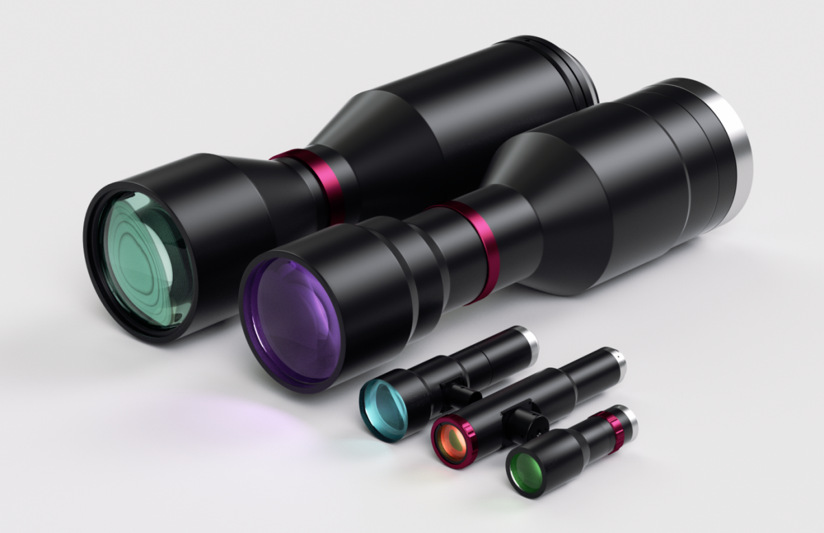
Lenses
The system’s lenses focus the product’s reflected light onto the camera’s image sensor. To get clear photos, you need to have a collection of high-quality industrial lenses.
The image resolution of the AOI device determines the precision of information it can detect and record. In other words, resolution is crucial since it determines how quickly and precisely an examination can be performed.
Remember, the CCD imaging system is the foundation of the AOI system. The light source typically highlights the components under inspection. However, the important task, i.e., taking the picture, is performed by the lens, which then transmits it as a beam of light to the sensor. The quality of a pixel, or the quantity of information contained in a pixel, is mostly determined by the camera’s lighting system and lens.
That’s why it is highly important to choose a better lighting system and advanced lenses. After lighting source, the success of your inspection operation depends on the type of lens you choose.
Camera
The digital camera usually takes a picture of the product. AOI systems can use everything from simple 2D cameras to highly advanced 3D sensors. They receive light and transform it into digital data in millions of small cells called pixels. Algorithms inside the AOI’s software then use this information to do the inspection.
AOI 3D systems allow for rapid, comprehensive examination of complete circuits, vastly improving the efficiency and precision of quality control processes. Thus, you can rest assured that only the best quality items will leave the factory. The cutting-edge AOI technology can spot flaws that would otherwise go undetected by human inspectors.
If you use AOI 3D as part of your quality control procedure, you can be confident that your electrical devices will work as expected.
Final Thoughts!
Because of its lower production costs and shorter production times, SMT has replaced Through Hole Mounting. Now, SMT is the standard method of PCBA assembly in most electronics companies.
Moreover, electronic components have shrunk in size as manufacturers respond to consumer demand for more compact goods like mobile phones. Component assembly on circuit boards is one area that has evolved alongside other technological developments. Thanks to technological advancements, even little devices can now provide lightning-fast service.
Now is the time to leverage the power of optics, mechanics, and software. AOI is a cutting-edge technology that can replace human inspectors. As we know, even the smallest board might include thousands of soldered components in today’s competitive PCBA manufacturing environment. As a result, automatic optical inspection (AOI) is becoming more critical.
AOI technology helps businesses lower production costs, decrease waste, and increase yields by constantly assessing the quality of production while making adjustments to the process flow. Companies who want to improve their production skills and stay competitive in the market should consider investing in AOI systems.
One thing, though! When you plan to set up an AOI system in your production plants, make sure you support them with high-quality lenses. At VICOImaging, you will find a range of industrial lenses that are tailor-made to suit different industrial inspection operations. Our lenses improve efficiency while maintaining a high standard of quality. You can realize competence and cut down on wasted time spent on manual inspections by incorporating our optics into your manufacturing process.
Do you need guidance setting up the AOI system? Or do you need help picking suitable lens models for your existing AOI system? Make sure you get in touch with one of our executives.
