
Picking the best lens for wafer testing – things you should know
One of the biggest challenges of semiconductor wafer production is the QA. Flaw/defect inspection and testing for wafers usually happens on the micro level. Usually speaking machine vision, or computer vision as sometimes called, are involved in the process as the naked eyes just aren’t enough for inspection and are only (rarely) involved once the imaging process is done.
For any machine vision system fit for wafer inspection, the first thing you need to know is that:
- Wafer defects come in many different ways.
- They usually happen in a micro level.
This means that a defective wafer can be distorted, dent, discolored, cracked or scratched in a microscopic level that requires a specially-made industrial camera powered by AI algorithms to efficiently and accurately detect them. That requires the lens part to be high magnification:
- High magnification
- Highly customizable, because the working environment for each semiconductor assembly or testing workplace is different
- Long working distance, because the longer the WD the more freedom you have in designing the compact vision system.
- Large depth of field, a larger DOF ensures the lens won’t have layering issues when inspecting.
A compact machine vision system is the key for QA process in semiconductor production and picking the right lens is vital. In this article, we are going to dive in on one of the crucial parts of the system – industrial lens.
Read more: WH Series Lenses: Enhancing CoWoS Advanced Packaging Inspection in Semiconductors
First, what is a wafer?
According to Wikipedia, wafer is a special thin slice of semiconductor made for integrated circuits fabrication or solar cell production. Typically, any thin slice of semiconductor material is a wafer.

A thin slice of wafer (credit:www.seica.com)
Wafers are produced using a highly purified, single crystal material. For the Czochralski process, a cylindrical ingot comprised of a highly pure (99.9999999% or higher) monocrystalline semiconductor such as silicon or germanium is made by pulling a seed crystal from melting state. To appropriately dope the crystal, impurity atoms that act as donors are precisely added to the molten intrinsic material. This results in the transformation of the semiconductor into either an n-type or p-type semiconductor. Finally, the ingot is sliced to produce wafers. This process is named after its Polish inventor: Jan Czochralski.
Secondly, what is machine vision or computer vision?
Computer vision is an umbrella term used to describe utilizing artificial intelligence to process digital images, videos or other data in order to analyze meaningful information from them. It is widely used in automotive, robotics, medical imaging, semiconductors, manufacturing and many other industries. In a human body analogy, computer vision is the compound system of human eyes and brains, where the cameras serve as eyes, and AI algorithms serve as the brain.
But compared to human bodies, computer vision has many distinct advantages: Its data acquisition is much faster, more precise and has much more freedom in working distance than a pair of human eyes do. The AI algorithms also can work much faster and more reliably in learning, analyzing and memorizing data than a human brain.
Since wafer inspection requires visual analyzation on a micro level (way beyond the capability of naked eyes) and its detection accuracy demands precision within a millimeter, computer vision is widely used in this process.
And how can industrial lens help with wafer testing?
Since computer vision is about acquiring and analyzing visual data, it can boost both the efficiency and accuracy in quality control or inspection process in manufacturing tremondously, and wafer inspection is no exception.
The AI algorithms built in vision inspection system can process visual data and analyze them for flaws, such as tears, irregulars or discolors, which are common in wafer production, in a matter of seconds. This process allows for continuous production and inspections process without human intervention, saving both money and time, while increasing efficiency and reducing errors.
Just like a human engineer would do in inspection process, the machine vision inspection process consists of two steps: Imaging (the “seeing”) and analyzing (the “thinking”); the latter requires a stable software and computing power, together with an algorithm that has defining parameters for errors, like the diameters of irregularities, or chromatic data for discolors. The former, however, requires a high precision and customizable industrial camera. To get such a camera, first you need to decide its crucial part – the lens.
Read more: Scanning Defect Inspection
What qualities should you be looking for when picking lens for wafer testing?
When you build a vision system for quality control purposes, industrial lens is one of the most crucial parts. There are various deciding factors of a lens that can impact your efficiency in wafer inspection. We have previously made a lengthy guide on how to pick industrial lens but to tell a long story short: Magnification, FOV, telecentricity and working distance are the key factors. Beyond that, you also need a high-resolution camera compatible for the lens.
For wafer inspection, it is recommended to have customizable magnification and working distance of the lens, this is due to wafers might come in different size and inspection area; the customized working distance also allows you to put together a vision system that can work in different scenarios without needing one system for one specific scenario only.
You might also want to look for an industrial lens with a large FOV and/or DOF, this is because when paired with longer working distance, a lens with a large FOV and/or DOF can achieve a certain flexibility in compact vision system without losing any precision or accuracy, especially in layering precision.
Read more: WH Series Lenses: Enhancing CoWoS Advanced Packaging Inspection in Semiconductors
Different types of wafer testings and their most suitable lens
Generally speaking, wafer defects happen on two scales: macro scale and micro scale. Machine vision solutions are usually utilized for micro-scale defect detection.
So what are the types of wafer testing in machine vision inspection? Well, there are:
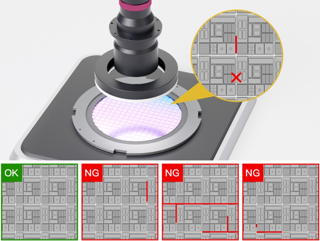
Parameter inspection: This wafer testing involves inspection of the workpiece dimensional parameters such as width, length. The vision system would take the imaging data, run it through its algorithms, and test if the parameters are within acceptable range.
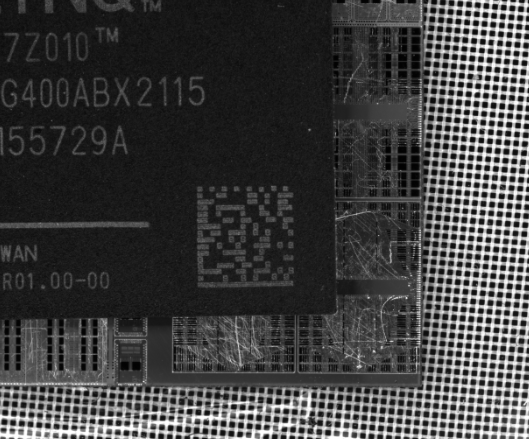
Surface inspection: Wafer surfaces can be tested for any anomalies such as dent, scratch, crack, foreign particles, peelings or misalignment. This process requires the lens to have high precision and magnification so that any small, microscopic level of imperfection would be detected by the algorithm.
As mentioned earlier, picking a highly customizable lens with a long working distance and large DOF is recommended be cause it helps your industrial camera, along with the rest of the computer vision inspection system, to suit various working conditions so that you don’t need to build one for each scenarios.
Furthermore, a lens with long distance WD also allows your inspection workpiece to be a bit further than regular lens, while maintaining a larger FOV or DOF.
This gives the lens the ability to focus on a larger area, covering more wafer surfaces while effectively detecting any angular or spots irregularities.
A long distance WD lens are also the most cost-efficient industrial lens, given the fact that they are the most customizable and compatible which allows you to easily integrate them into your vision system.
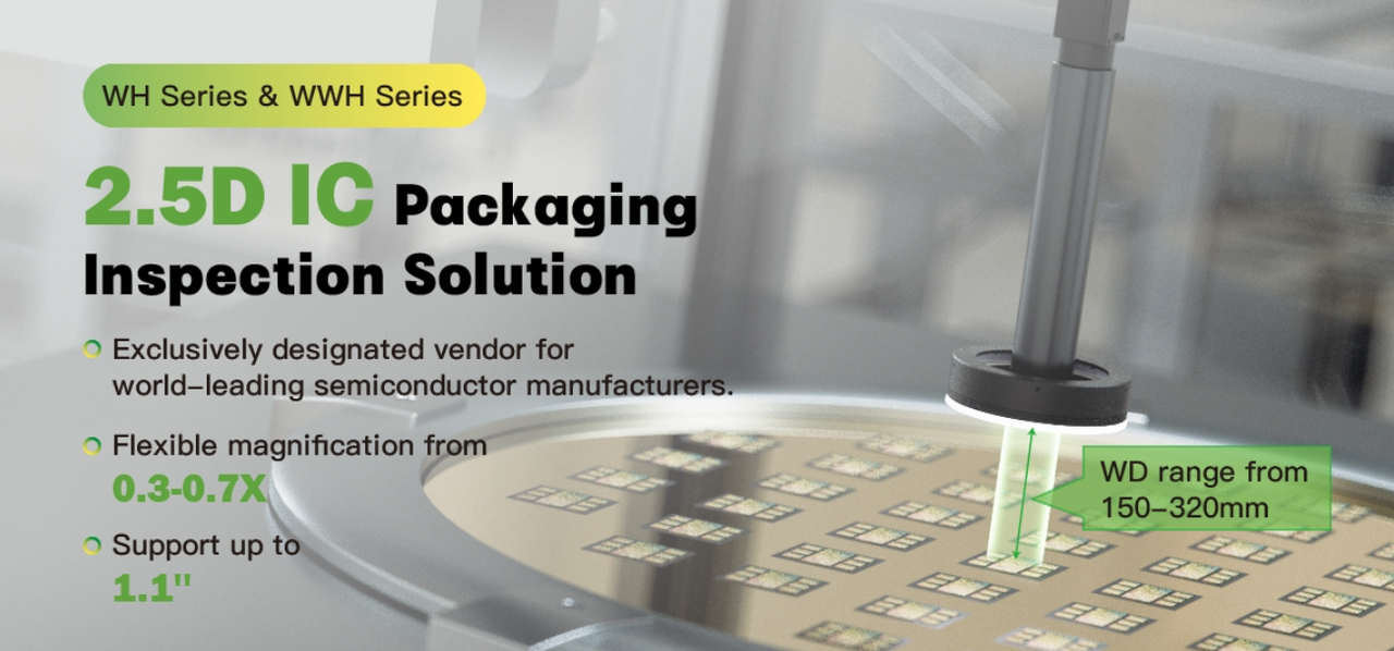
Read more: WH Series Lenses: 2.5D CoWoS IC Packaging Inspection Solution
In conclusion
Wafer defects that happen on a micro level are best detected by computer/machine vision system, which are faster, more precise and more efficient than human inspection. But picking the right lens for the vision system is crucial, and you mostly would like an industrial lens that has long working distance, high magnification and larger DOF.
Such a highly customizable lens allows you to easily integrate it into your vision system, which can be used in various working scenarios, so you don’t have to build a camera system for each special working environment.
Tip: Check out our WH series.
