
Space management on the PCB may often trigger incorrect component placement in today’s age of downsizing PCBs. Correctly placing components on a PCB enhances the product’s signal quality and functionality. From the PCB assembly perspective, proper part placement minimizes manufacturing expenses. It also shortens project timelines for production and improves performance. Thus, planning to place components on the PCB is an essential step in the design process.
For this, 3D Automated Optical Inspection (AOI) systems have emerged as a crucial tool for the Surface Mount Technology (SMT) and Surface Mount Device (SMD) sectors. Since these technologies provide supreme dependability to maintain high-quality boards with many solder connections, their significance to manufacturers has grown.
But does this imply that every 3D AOI can act as a failsafe system to catch issues early on? In specific cases, it can be yes, while in others, no. Authentic 3D-based systems often surpass various challenges that ordinary optical inspection systems confront due to the shrinking of components.
This article provides an operational and manufacturing perspective on the importance of component placement. In addition, how the 3D AOI system and its features can aid in more precise PCB construction.
What Does SMD Stand for in Electronics?
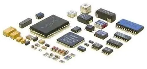
SMDs, or surface-mount devices, are the parts that go onto a PCB. In this era, companies are continuously looking for more efficient technologies, like SMT and SMD. The new SMDs have pins that can be soldered right on the PCBs, replacing the earlier method of wiring the SMD onto the boards. Now, SMD allows you to use smaller components while achieving the same performance.
If that’s the case, components can not only be compact, but they can also be multipurpose. Since no drilling is required, the whole process is quick and cheap, allowing for additional circuits to be provided on the board.
Moreover, it provides superior high-frequency performance with fewer side effects from RF signals. In addition to being more cost-effective than devices that need drilling a hole, SMD’s portability and ease of use also make them a better value. Miniaturization, the absence of any kind of lead, and compatibility with surface assembly on PBC are all notable aspects of the SMD.
Also Read: The Basics of SMD and SMT: A Comprehensive Guide
What Is the Difference between Active and Passive SMD Parts?
SMD soldering often employs capacitors, resistors, ICs, and inductors as its parts. They are available in a wide range of forms, including QFPs, BGAs, and rectangular packages. Active and passive components together make up the SMD.
Active Components
To carry out their intended task, active components need to be supplied with energy, usually a direct current. These components can control the flow of power. Diodes, transistors, and integrated circuits are a few examples of semiconductor devices that comprise most active components.
- Transistors
It is one kind of semiconductor device. It acts as the supporting block of the electrical architecture of phones, computers, and many other gadgets. Oscillators, amplifiers, voltage regulators, modulators, and switches benefit from the quick reaction time of a transistor.
- The Integrated Circuits
These are a collection of electronic components packaged together. The shapes and sizes of IC packages vary widely.
- Diodes
A diode is like a one-way electrical switch. It often includes a painted line at one end to indicate which way the current should travel.
- Op-Amps or Operational Amplifiers
Applications, including audio systems and control circuits, use SMD op-amps for signal conditioning, amplifying, and filtering.
- Sensors
SMD sensors can detect and measure a wide range of factors, from temperature and pressure to light and motion. The electrical signals derived from these observations have several uses.
Passive Components
As their name implies, passive devices do not amplify or increase a signal. Passive components can’t create, oscillate, or amplify an electrical signal. Instead, it can solely act as a receiver, dissipating, absorbing, or storing the energy it receives in the form of an electric or magnetic field.
- Resistors
The purpose of a resistor, in electrical terms, is to slow down the flow of electricity. It’s a passive component in an electrical circuit that creates a voltage drop across itself in order to regulate the flow of current through the circuit.
- Capacitors
Simply put, a capacitor is a passive electrical part that stores energy as an electric field between two conductors. Charging refers to the action of transferring energy into the capacitor. Likewise, capacitance is a quantitative measure of a capacitor’s charge-holding capacity. Electronic circuits rely on capacitors because of their ability to store energy temporarily.
- Inductors
You can also get inductors in the form of a chip. However, it is impractical to manufacture chip inductors with high values. This component is more like a magnetic energy storage device that only allows for the passage of direct current (DC) and not alternating current (AC).
- Transformers
The next example of a passive electronic part is a transformer. In spite of the fact that transformers are often employed to increase voltage levels, this is not the case since it keeps the power constant.
What Are the Advantages of SMDs in High-End Products?
- Thinner and More Compact PCB
Surface-mounted devices (SMDs) are typically 60-80% less in size compared to their counterparts. There is also a considerable reduction in the weight of these parts. For this reason, they contribute to the SMT PCB’s tiny stature by taking up less room there.
- Improved PCB Flexibility
Surface Mount Technology’s ability to mount or solder SMD components directly to the board’s surface is incredible. It makes the board’s material and design highly adaptable. SMT is what makes Flex PCB and Rigid-Flex PCB a reality.
- Reduced Material Cost
It can save money on raw materials since through-hole plating is unnecessary. Many surface-mount electronic components are cheaper than their through-hole counterparts. Thus, it aids in decreasing the price tag associated with making SMT PCBs. Because of their compact dimensions, Surface Mount Assemblies save money on packing, shipping, and handling.
- Automated Simplification of Production
Leads of through-hole electronic components need manual insertion into plated through-holes. You’ll need to cut, shape, and bend these leads. The Automatic SMT Pick and Place Machine allows for hands-free placement of components directly onto the PCB. In turn, this lowers manufacturing and processing costs.
- High Signal Transmission
SMT PCB Assembly can handle high density, especially on double-sided PCB and multilayer PCB, which are ideal for high signal transmission and high-frequency applications. These boards can transmit signals at fast speeds since there is little latency. SMD components also have less RF interference since they have no leads or very short leads.
What Are the SMT Manufacturing Processes?
Printing solder paste, placing components, and reflow soldering are the three main steps in the SMT production process. However, the following overview delves further into these phases and explains the specifics of the SMT manufacturing process.
PCB Layout and Design
Choosing the SMCs and designing the PCB are the first steps. Solder pads are flat. They are often silver, tin-lead, or gold-plated copper pads on the board that are free of holes. The pins of parts like transistors and chips rest on these solder pads.
Solder paste printing follows the placement of solder pads on the PCB. Therefore, the stencil is essential for keeping everything in its proper place. All of the raw materials and parts that will go into a product must be thoroughly inspected before production can begin.
Solder Paste Printing
It is an essential step in the SMT procedure. Employing the previously created stencil and squeegee (a tool for cleaning in printing), the printer applies solder paste at an angle of 45° to 60°. Putty-like solder paste is a combination of solder powder and a sticky flux. Flux acts as a temporary adhesive to keep surface mount components in place and removes contaminants and oxidation from soldering surfaces.
Solder paste is what links the SMC to the PCB’s solder pads. Each pad must have an adequate coating of paste, which is why this step is so crucial. If not, it will be challenging for the reflow oven to melt the solder.
Reflow ovens are electrical heating devices used in surface mount technology (SMT) in the electronics manufacturing sector to install electronic parts on printed circuit boards (PCBs).
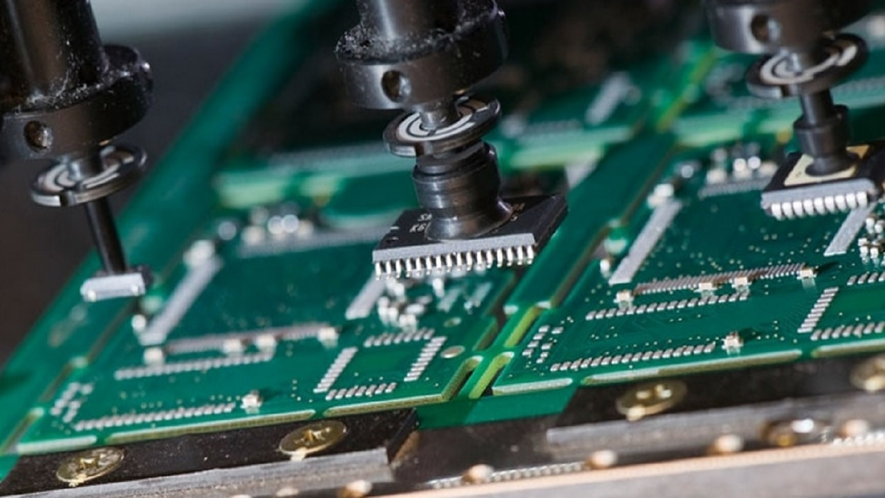
Arrangement and Placement of Components
The next step is to put components on the PCB using the pick-and-place machine. The placement machine comes with a vacuum or gripper nozzle. It helps the machine to extract each component from the package. After that, the machine places it in its designated spot.
Some of the fast and precise machines can install as many as 80,000 tiny parts per hour onto the PCB as it moves down a conveyor belt.
Solder Reflow
Following the placement of SMCs, the PCB is sent to the reflow soldering oven, where it travels through the following zones:
– Preheat Zone: In the first part of the oven, called the preheat zone, the circuit board and all its associated components are heated gradually yet uniformly. Until it reaches 140°C – 160°C, the temperature is increased at a rate of 1.0°C – 2.0°C per second.
– Soak Zone: In the soak zone, the board will be heated to between 140 and 160 degrees Celsius and held there for 60 to 90 seconds. After entering the reflow zone, the boards are heated to a maximum of 210°C-230°C. It melts the tin in the solder paste and fusing the component leads to the pads on the PCB at a rate of 1.0°C-2.0°C per second. The surface tension of the solder keeps the parts in place while this is happening.
– Cooling Zone: The last step is a cooling zone, which ensures the solder solidifies once it leaves the heating zone. If the PCB is double-sided, you may use solder paste or adhesive to secure the SMCs on both sides.
Cleaning and Inspection
Cleaning and inspecting the board for defects is the next step after soldering. If flaws are discovered, companies often prefer to either fix them or put the product away. High-quality industrial lenses, AOI (Automated Optical Inspection), flying probe testers, X-ray inspection, etc., are common tools used for SMT inspection. The usage of technology has replaced human involvement because of the speed and precision it provides.
What Are the Applications of SMD?
SMDs are used in many different fields, including consumer electronics, automobiles, industries, healthcare, and communications.
– Consumer electronics typically use them to reduce the size and weight of parts, which can lead to cost savings.
– Increasing heat dissipation and decreasing component size are two common uses for them in automobiles.
– Industrial uses, such as semiconductor making, often use SMDs in high-temperature environments.
– Their small size and increased reliability make them a popular choice for use in implanted medical devices.
– Finally, SMDs are widely used in the telecommunications industry because they allow for a greater density of components on smaller circuit boards.
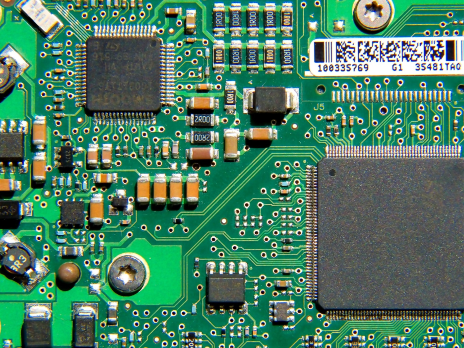
What Are the Requirements for Component Placement in SMD Assembly?
Component placement is one of the initial steps in PCB design, yet it requires extreme caution to minimize the need for expensive rework and time loss. The following guidelines are the backbone of every PCB designer’s toolkit for achieving component placement perfection.
Classify Parts by Their Intended Use
It’s important to categorize components according to their shared purposes. Power management ICs (PMICs) and other high-heat-generating, high-current devices like converters and LDOs belong together in the equivalent power management category.
If the analog and digital components employ signals with high switching frequencies, the power supply should be located in a separate area. It is also important to isolate components that produce electromagnetic noise or radiation from components handling more delicate signals.
Keep the Parts in a Consistent Orientation
A reference pin is present in every integrated circuit, no matter its size or number of terminals. Designers must ensure the ICs are all facing the same way to facilitate the PCB layout and save assembly time. It improves assembly throughput and cuts down on misaligned parts.
When soldering, it is best practice to align components with the same orientation, which also applies to passive components. The recommendation is to arrange the parts in rows and columns (a kind of matrix) with a consistent orientation to facilitate inspection and maintenance procedures and pick-and-place machine assembly.
Electrolytic and tantalum capacitors, as well as diodes, are polarized components that must all be installed with the same orientation. The recommended minimum distance between components is 40mil, while the minimum distance between components and the PCB edge is 100mil.
You should also keep components away from through-hole connections on the solder side of the PCB. If you want to make assembly easier, put all of your surface mount (SMT) components on one side of the board and your through-hole components on the top.
Create Separation between Various Sections
It’s important to divide the printed circuit board (PCB) into distinct regions for the many types of components it will house. With their respective functions isolated, analog and digital signals are less likely to cause harmful crosstalk occurrences and disrupt one another.
Keeping non-homogeneous components in distinct regions is the easiest method to avoid overlapping analog and digital traces. Use the component’s function and the maximum safe voltage and current levels as partitions.
Don’t Place Components near Heat Sources
IGBTs, PMICs, MOSFETs, and even voltage regulators generate considerable heat in high-power applications. Although adding vias between components may help with heat transfer, keeping non-power components at a safe distance from the power components is still desirable. The same holds true for thermally active components such as operational power amplifiers.
Allow Enough Room for the Traces to Appear
The need for smaller printed circuit boards (PCBs) is a current trend in electronics, especially in the wearable and handheld gadgets industry. Still, there’s only so much you can do to shrink circuits, and there’s always the best size to aim for. Otherwise, following their paths becomes quite difficult. Therefore, it is important to provide enough room on the PCB for the routing of copper traces while placing the components, particularly near components with a large number of pins.
What Is the Impact of Component Spacing on Thermal Management?
When deciding where to put parts, it’s important to factor in how hot they’ll become under normal conditions. The central placement of heat-generating components promotes uniform thermal dissipation throughout the PCB.
It is also important to consider the direction the airflow will take to ensure that the largest components won’t get in the way of the cooling of the smallest ones. Increasing the space between components improves the PCB’s heat transmission and makes the board safer to use. It helps you stay away from common PCB design pitfalls like thermal hotspots. Remember, having powerful components so close to the edge generates a lot of heat.
The Importance of 3D AOI Lens in Addressing the above Applications and Problems
Both bare board PCBs and PCB assembly processes can benefit from AOI. Depending on the details you need and how quickly you need them, many process engineers choose post-reflow AOI.
In short, AOI must be able to inspect yield rate, dispersed defect type, total number of flaws, etc. It should also help with the recognition of barcode information, measuring or gauging, package size, and lead condition.
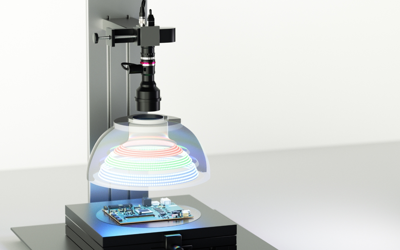
Describe a 3D AOI System
As ordinary AOI technology has progressed, so too have three-dimensional AOI systems. These systems create a precise map of the object under inspection using 3D imaging technology, often based on laser triangulation or structured light projection.
Laser Triangulation
Putting a laser line onto the object’s surface and photographing the resulting triangular pattern is the essence of laser triangulation. The system can estimate the surface’s height profile by examining the distortion in the line. This technique is so accurate that it can measure heights with around 1-micron resolution. But it’s slow since you have to move the laser line over the whole object.
3D AOI with Structured Light Projection, Cameras, and Lenses
Structured light projection is the best alternative to the time-consuming laser triangulation method. This technique works by projecting an arrangement of light onto the object’s surface and taking a picture of the distorted pattern. The system infers the topography of the surface from the degree of distortion in the pattern. The usual height resolution of this approach is roughly 10 microns, making it quicker as compared to laser triangulation.
Why Choose 3D AOI Lens System?
Its algorithms are very accurate and can identify even the most subtle of flaws. The volume and shape-related flaws in components and solder connections are some of the easiest for 3D AOI systems to spot, which is one of their key benefits. For instance, a 3D measuring system can do what no other inspection system can, like accurately gauging the volume of a solder junction and determining if it is enough or excessive.
Another perk is that differences in lighting and part color have less impact on 3D systems. Their increased durability and adaptability mean they can check a wider variety of parts without having special settings for each color or material.
The Advantages of 3D AOI Systems over 2D AOI Technology
When it comes down to comparison, 3D AOI inspection is just a more advanced optical inspection system with built-in measurement capabilities. Due to the inherent challenges of 2D inspection systems, height measurements are not readily detectable, making 3D inspection the sole viable option for measuring inspection criteria such as solder fillet, coplanarity, tombstone, and IC lift.
The high dynamic range of the 3D AOI system allows for the extraction of component and solder junction shapes as well as the detection of any flaws. All inspection findings rely on either contrast or position of reflection spots since 2D systems release light from many angles onto the PCB, components, and solder connections. Light availability still determines the final product, regardless of the number of cameras, lenses, or viewpoints employed.
Thus, components with a greater height will throw shadows on neighboring components and solder joints. Due to shadowing’s effect on illumination, the AOI programmer must adjust thresholds separately for each component.
Also, different defect detection capabilities and various numbers of false calls result from using different criteria for the same kind of components on the same board. Alternatively, you might adjust the inspection software to take additional photographs, such as from right above the examined component to prevent the shadow effect.
A 2D or 3D AOI system may be preferable depending on the task at hand due to differences in available technology. However, you should also think about the PCB assembly’s budget and its intended function. Where standard 2D AOI inspection lacks the measuring capabilities necessary for quality assurance, 3D AOI technology steps in to fill the void.
The use of a 3D AOI system is the best method for improving product quality via process optimization. An established EMS that provides SMT assembly for competitive markets would most likely choose to use such a solution.
3D AOI Implementation in Production
When it comes to maintaining the quality of goods, automated optical inspection (AOI) is crucial, especially in the electronics industry. To reduce the likelihood of subpar goods, companies can use a 3D AOI system to detect flaws in the product at an early stage of manufacturing.
The Function of 3D AOI in Quality Assurance
The quality inspection process is where 3D AOI is most often used to find manufacturing flaws. Automated optical inspection (AOI) systems are crucial in today’s high-speed production lines because of their accuracy and efficiency. 3D AOI systems can find a wide variety of flaws, such as improper polarity or soldering, as well as misaligned or missing components.
Moreover, 3D AOI facilitates early detection and correction of production faults, minimizing material waste and the need for costly rework. Also, 3D AOI systems can give helpful information for controlling and improving the process.
Manufacturers can now identify problem areas and make improvements to prevent similar problems in the future. Industries, including consumer electronics, automobiles, and aircraft, rely heavily on 3D AOI for quality control because of their tight requirements.
Use of 3D AOI in High-Speed Production Lines
A high-speed production line must be able to keep up with demand without compromising product quality. Due to the high volume and rapidity of such lines, human inspection is typically insufficient. For instance, without machine vision, it might be very difficult to see microscopic solder bridges during board inspection.
With the right setup and components, a 3D AOI system can process hundreds, if not thousands, of parts per minute. This speed is proportionate with the output rates of modern, high-speed assembly lines. 3D AOI systems, for instance, are built to keep up with the high placement rates of contemporary SMT lines, which can position over 40,000 parts per hour.
In high-speed manufacturing, 3D AOI systems can detect faulty parts and provide immediate feedback to previous processes. If the 3D AOI system notices a trend of misaligned parts coming from a certain pick-and-place machine, it can quickly feed that information back to the machine, allowing the operators to make instantaneous adjustments to the alignment settings.
This capacity lessens the spread of defects and the associated costs of reworking or waste. The high-speed features of AOI also allow for more productive utilization of factory space. Checking items as they pass through the line is more efficient than stopping the line for human examinations or holding intermediate products for subsequent examinations.
The need for rapid production at a high level of accuracy and efficiency has led to the development of 3D AOI as a viable option. Many manufacturing processes will likely be automated in the future. It will make AOI integration even more crucial in the years to come.
Problem-Solving Capabilities of 3D AOI Lens in SMD Assembly
Some AOI suppliers only provide sparse 3D component coverage at best. Solder joint quality and production efficiency can both benefit from the use of genuine 3D AOIs. It offers comprehensive 3D coverage to aid in the detection of defective boards and the tracking of operational efficiency for manufacturers. In addition to spotting obvious flaws like missing or incorrect parts, 3D AOI systems can spot unnoticeable problems like coplanarity and lead bridging.
Solder Joints
The solder deposit changes with the board design. Also, solder joints often exhibit specular reflections, making solder junction measurement much more difficult than measuring a component body. These variations may interfere with the ability to visually detect flaws in solder junctions.
An algorithm in 3D AOI systems processes the collected data to provide reliable and consistent measurement data for the leads of resistors, capacitors, and other components. It provides this data irrespective of the number or form of solder joints.
Shadow Problems
Does precisely locating the body also ensure precise dimensions and measurement data? Certainly not! Even with top-notch inspection equipment, companies face a number of obstacles. The presence of shadows is a significant issue.
Some small components, such as resistors, might be obscured by taller nearby parts, like connectors, leading to flawed measurement findings when the board is built. 3D AOI can reduce blind areas due to the high-quality cameras and lenses it uses.
Optimizing Processes Using Authentic Information
Every company and equipment supplier, including those that provide automated inspection, strives for process optimization. It has proven challenging for 2D AOI systems due to a lack of height information, which prevents precise measurements of shape, coplanarity, and solder volume.
By measuring each side of the part and solder junction to the prescribed standard and generating a large collection of authentic measurement data, 3D AOI systems can overcome these obstacles.
Board Warpage
The inspection systems also have trouble with board warp. Pad locations described by board CAD or Gerber files seem warped on a warp board, which may throw off traditional inspection techniques and lead to inaccurate results. As a result of the high temperatures generated by the reflow process, the board warp grows more prominent.
Even with high-quality components, the board warp causes inconsistencies in component height. For this reason, 3D AOI systems use a robust algorithm to actively adjust for warpage.
Inter-Reflection Problems
Inter-reflection is another major problem. Components on completed circuit boards with solder and tin plating may have specular surfaces that strongly inter-reflect with other light reflections. Thus, these components reflect part of that light back to the camera. They distort the height measurement result because part of the reflected light fails to hit the camera.
As board density rises and component spacing falls, the problem of specular reflection becomes more acute. The 3D AOI gets over this problem with its high-quality multi-view sensors and stops measurement errors with its cutting-edge 3D image fusion technology. The 3D AOI uses multi-projections and sophisticated algorithms to accurately detect and filter out the many reflections created by bright components and solder connections.
Speed and Inspection Consistency
Another problem with inspection systems is the lengthy cycle time required to scan millions of pixels in order to rebuild complete 3D pictures from fresh data acquired through numerous channels. Unlike 2D AOI systems, 3D AOI systems will never sacrifice accuracy for speed. These systems use cutting-edge optical technology and cutting-edge hardware, so they consistently provide accurate results.
Final Thoughts!
Using surface mount technology (SMT), electronic components like transistors, resistors, integrated circuits (ICs), etc., can be soldered straight onto the surface of a printed circuit board (PCB) during the electronics assembly. However, SMT is not a zero-defect process. As components get more miniaturized and PCB area density increases, it becomes increasingly difficult to rectify possible faults, particularly if the defect is discovered at the last stage of assembly.
Implementing strict quality inspection is crucial for preventing such adverse mistakes. It verifies that the PCB assembly is free of flaws and ready to go on from the SMT assembly line. Obviously, in high-volume manufacturing lines involving complicated electrical devices, manual inspection is not the best option. The primary reasons are the excessive cost of the PCBA examination and time requirements.
Using 3D AOI systems, PCB assembly companies can pinpoint faulty boards by precisely positioning individual components. It prevents costly sequential mistakes from occurring and lowers the overall cost of repair. Additionally, it improves the standard of future production runs. The speed of this technology also boosts the system’s overall efficiency and output.
So, make sure you invest in a high-quality 3D AOI system, especially when your manufacturing needs are higher. With 3D AOI systems, there comes a need for high-quality cameras and industrial lenses. In fact, the whole performance of 3D AOI systems depends on the cameras, lenses, and software.
Are you struggling to get a reliable 3D AOI system for your production lines? Do you have no idea about the type of lens to pick for your system? Don’t worry! You can contact VICO Imaging to get industry-specific guidance from the experts.
