
Factory Automation (FA) is everywhere in today’s industry 4.0 world, and semiconductor field is no exception. With the new trend of 2.5D/3D IC packaging and wafer testing while stacked, the technologies and requirements have been pushed to a new extreme.
It’s not the traditional methods and equipment wouldn’t cut it. But they require too much attention and manual adjustment to really fit in a modern semiconductor manufacturing environment where few to none human workers on site were involved. In fact, Samsung just announced that they are going to start building all-AI, no human chip factories.
Most of the human involvement in wafer handling and inspection/QA processes, for example, have been done by robot arms. Compact solutions that involve robot arm, computer visions and PLC have been the trend for quite a while for industry leaders.
But building such a system is no easy task, there are a lot of factors to decide for maximum cost-efficiency. For example, one thing that many wafer/IC testing companies are worried about space-saving when incorporating computer vision into their 2.5D/3D inspection process. Typically, a robot arm (or even several) is responsible for handling the workpiece, but since an industrial camera is needed to acquire visual data for inspection, the working distance of said camera needed to be exceptionally long to allow room for the robot arm to go though. Another thing is the DoF of said camera needs to be larger than traditional cameras to allow proper imaging when inspecting stacked IC dies, because the stacking produces a difference in the distance between various workpieces and the lens, especially so in 3D packaging where the stacks could be 4 or even higher. Without a lens with larger DoF, manufacturers would have to manually adjust the imaging circle to inspect between IC dies, which would defeat the purpose of a modern semiconductor FA.
In this article we will discuss a few things about how to design a modern 2.5D/3D wafer/IC FA system. First, let’s go through a couple of basic concepts:

Read more: https://howtorobot.com/expert-insight/robotic-arms
Robot arms in industry 4.0
Industry 4.0 is a new revolution featuring the organic merge of digital technologies and traditional manufacturing. The major theater of this revolution is the industrial robot arm, for they redefined how manufacturers operate, and shaped the future of factory automation.
Robot arm acts as the bridge between physical production and digital information. These arms are “armed” with revolutionary sensors and software, making sure they collaborate seamlessly with their human co-workers, other compatible systems or even other robot arms. Compared to their traditional counterparts, they bring unparalleled precision, efficiency, flexibility and maxed-out repetition capability.
But for the robot arm to “see”, they need to have eyes, that is where the industrial lens come in. In this article we will explain the features and issues that come with industrial lens for robot arm.
Robot arm acts as the bridge between physical production and digital information. These arms are “armed” with revolutionary sensors and software, making sure they collaborate seamlessly with their human co-workers, other compatible systems or even other robot arms. Compared to their traditional counterparts, robot arm bring unparalleled level precision, efficiency and flexibility to the table.
First, let us dive in on the question of:
What is factory automation?
Factory automation (FA) is the manufactory process that is both executed and controlled by machinery, electronics, computing programs or other advanced technologies. Compared to traditional manufacture that is powered by human labor, FA is significantly better in efficiency, low errors, low maintenance and higher production quality.
FA is widely seen in manufacture, especially in automobiles, electronics, food & beverages, chemicals, oil and many more fields.
Main features of FA:
1. High efficiency: FA systems can repeat complicated process in high speed, greatly boosting production efficiency.
2. Consistency: FA ensures the consistency of product specifications by eliminating human interference and errors.
3. Low cost: This might seem counter-intuitive as the initial investment of a FA system can be substantial, but its cost-efficiency starts to ramp up the longer the production process goes as the maintenance of FA is significantly lower than that of human labor production.
4. Flexibility and expandability: FA is unique in that it is programmable, and therefore it can be adjusted according to production requirements with great flexibility.
5. Safety improvement: FA allows robot arms or robots to perform tasks that are usually highly risky for human laborers.
Some commonly seen FA components:
1. Sensors and actuators: Used for sensing environment variations such as temperature, pressure, visuals; as well as executing maneuvers.
2. PLC (Programmable Logic Controller): To control various industrial processes and machinery.
3. SCADA (Supervisory Control and Data Acquisition): To supervise manufacture process remotely
4. Robotics technologies: For tasks that are complicated, intricate or too high risk for human laborers.
5. Human machine interface (HMI): Allows operators to interact with automated systems to supervise and control manufacturing processes.
6. Industrial network and communications: For connections between various devices and systems, to make sure real-time data transfer and analysis possible.
7. Data analysis and algorithm optimization: Improve and optimize manufacturing process by acquiring and analyzing data.
Different types of robot arms deployed in FA
Robot arm is a mechanical device commonly deployed in FA, they could be automated or manually controlled.
Robots, on the other hand, is an entirely self-driven device which includes robot arms.
A robotic arm is a fixed or mobile device and is usually composed of a series of interconnected or relatively movable parts used to grab or move workpieces and are capable of executing automatic, programmable repeating process; They usually have multiple dimensions of motion freedom (axis). By making linear movements along the X, Y, and Z axis, robot arms are able to execute pre-programmed actions or reach the target position.
Robot arms are the most deployed type of robot application in manufacturing, medical appliances and even military and space engineering. There are 4 axis/5 axis/6 axis robot arms and 3D/2D robots; one thing in common is that they can receive data/command input and execute tasks in a 3-dimentional space with pin-point precision.
Robot arms and space-saving in semiconductor FA
Robot arms are massively deployed in place of human labor to minimise damage, misposition and containmination in modern semiconductor FA process. This is further enhanced by the fact that the current demand for semiconduct is surging thanks to the AI boom so major players in this industry are streamlining their FA and trying to meet the ever increasing quota.
In a typical semiconductor FA scenario, the production system can be quite compact: Multiple robot arms are designed for various tasks such as wafer handling, transfer, inspection/testing/imaging, segmentation or other. Engineers and PMs usually have to design carefully for space in order to achieve maximum cost efficiency and production capacity.
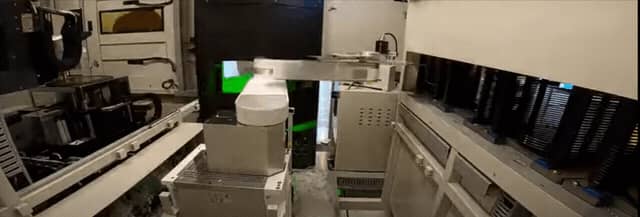
Notice on the top left corner where the industrial camera is located, it has a long WD to allow the robot arm to transfer inspection workpiece
For inspection process, computer vision technology is the primary player. We have made a previous guide on machine vision inspection process but the general idea is to use machine to replace human eyes, hands and brains with industrial cameras, motion devices and processing AI: cameras are in charge of capturing visual data which were then transferred and analyzed by AI algorithm to detect any defect or anormalies. For computer vision inspection to be effective and precise, the industrial lens is one of the crucial parts.
The key qualities of industrial lens for semiconductor FA
1. Extra long working distance
Given the fact that semiconductor FA has compact working space, the industrial lens in this scenario has to be customized to allow robot arms to fit in between the inspection camera and the workpiece, this requires the industrial lens to have extra long working distance while maintaining its high quality resolution to allow the AI algorithms to inspect defects efficiently.
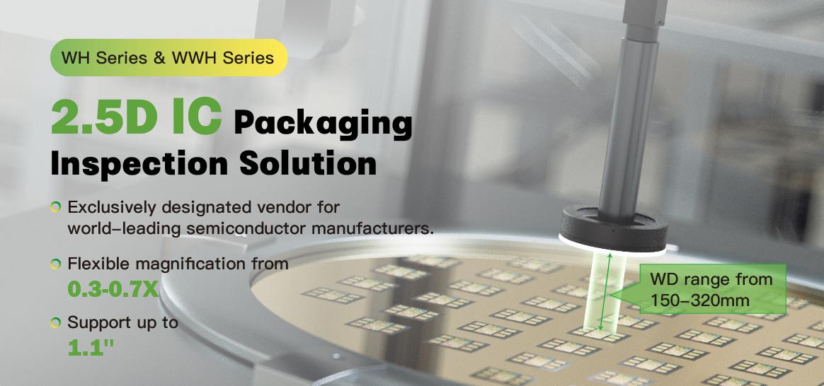
Read more: WH series with up to 1405mm working distance
2. Larger DoF
DoF (Depth of Field) is crucial for an industrial lens when it’s inspecting various objects with varying distance to the lens. We have explained different parameters when selecting industrial lens including DoF in a guide before, but to simplify: Depth of field is the parameter that the different objects in different distances to the lens can be focused without losing image quality. Larger DoF allows the lens to efficiently inspect defects on different IC dies/wafers stacked together in 2.5D/3D packaging simultaneously without the need to be manually adjusted. Not only would this allow the working environment to remain completely no human and thus reducing risks, but it also increases production capacity.
Furthermore, a larger DoF lens allows more customizable FA solutions, giving engineers more room to design their vision inspection system and thus greatly reduce equipment cost.
Read more: How WH series lens helped in CoWoS
3. Ultra high resolution
Ultra high resolution is crucial for industrial lens to properly inspect micro LEDs, semiconductors, PCB circuits or many other micro electronics.
High resolution, together with long WD and low chromatic abberation, is often regarded as the ideal industrial lens for inspecting semiconductors, especially for defects such as discolor, misposition, crush or dent, etc.
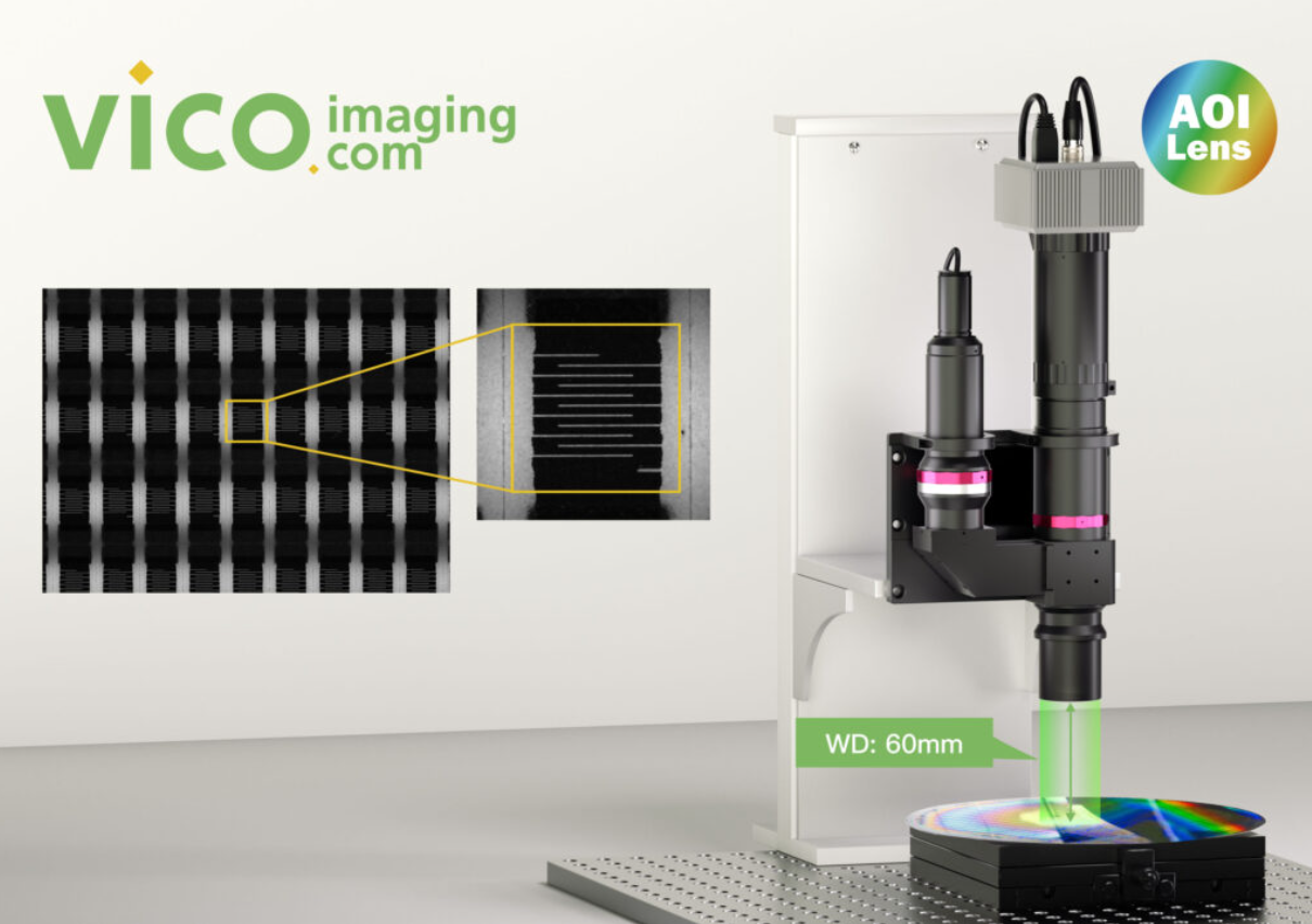
Read more: 1μm Ultra-Resolution AOI Lenses for Wafer Inspection
Conclusion
2.5D/3D wafer packaging is the cutting edge technology for maximum heat efficiency and performance. With this new packaging, the inspection process is required to evolve as well, especially so when major players in this industry are trying to go for all AI, no human working environment to reduce risks.
To allow for a compact FA system including robot arms, industrial lens/camera need to be designed to have longer WD, larger DoF while maintaining ultra high resolution. Not only would this allow for maximum amount of robot arms or other components, but it also greatly reduces cost. The lens with such key qualities would also be more suited for 2.5D/3D packaging since the stacking methods would create varying distances between the IC die and the lens.
