
In our first sneak peek, VICO Imaging will showcase innovative machine vision solutions for semiconductor applications. We present our COOLENS® WH, WWH, and WWK series telecentric lenses for die inspection, demonstrating their large DoF and precision in imaging tiny and multi-layered dies. In addition, our TUH series, as an industrial telecentric microscope lens, is featured in applications of the wafer surface and dicing kerf defects inspection, showing their exceptional performance in recognizing subtle defects. Our first sneak peek shows our devotion to advanced machine vision technology.
Exploring COOLENS® Telecentric Lenses for Precise Die Inspection
Issues
- Limited space for robotic arms.
- Difficult to strike a balance between large DoF and high precision.
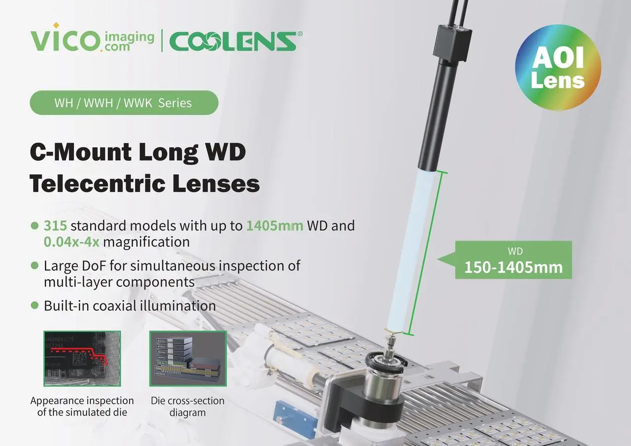
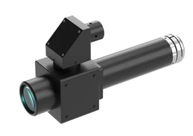
Highlights of C-Mount Long WD Telecentric Lenses
VICO Imaging has launched the C-mount long WD telecentric lenses to solve these issues. Long WD increases more room for robotic arms. Besides, our lenses can inspect multi-layer dies simultaneously with clear imaging for their large DoF, high telecentricity, and low distortion.
Key advantages:
- 315 models, 150mm-1405mm WDs, and 0.04x-4x magnifications for your choice
- Large DoF for simultaneous inspection of multi-layer components
- Built-in coaxial illumination
Read related post> Introducing WH Series-A New Lens For A New IC Packaging Era
Solution
Configurations:
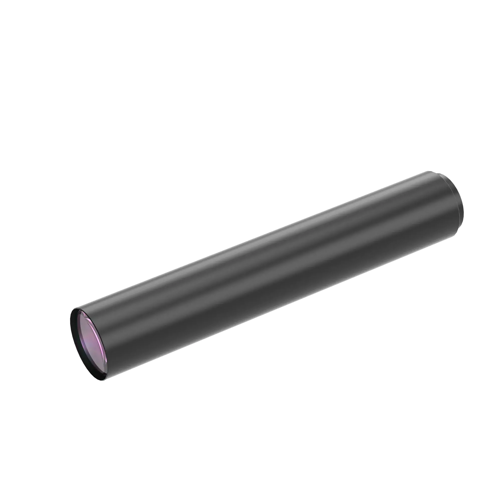
Lens: WH04-320A-111
Light: Shadowless white ring light
Camera: 2/3″ 5MP 3.45μm
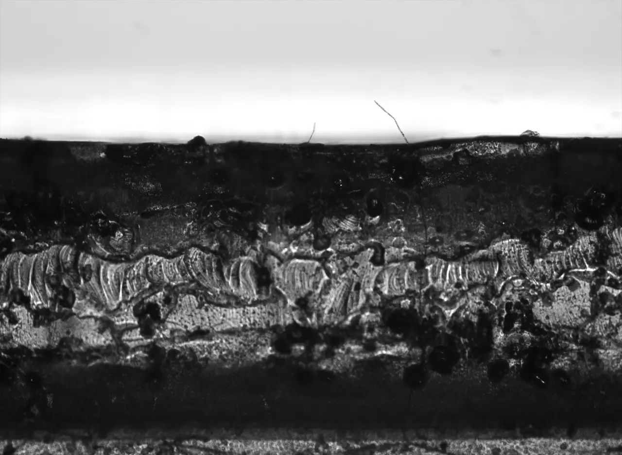
Results
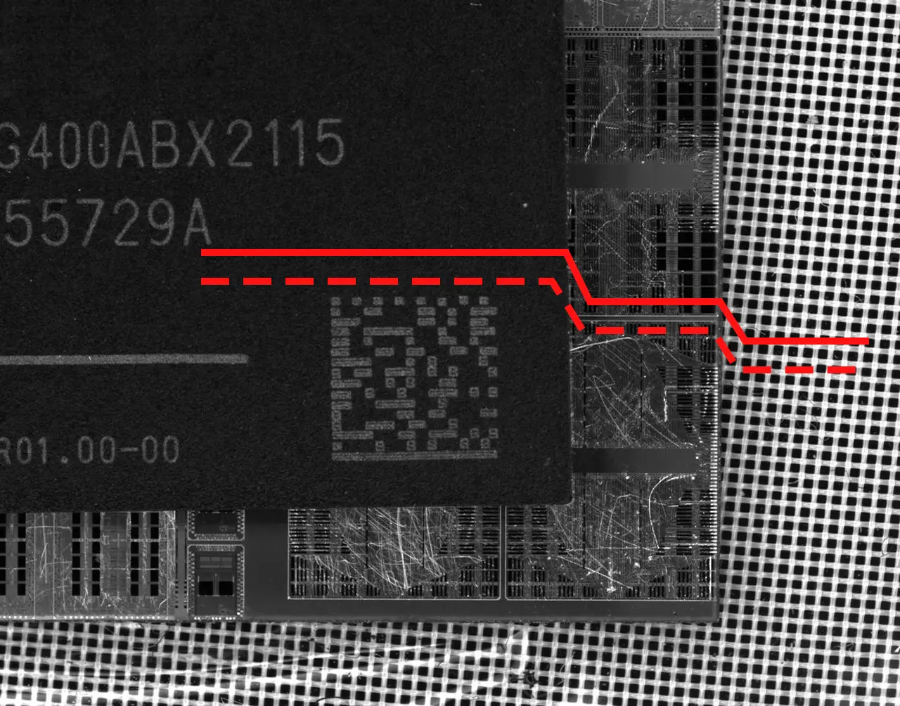
From the image of the simulated die inspection (on the left), subtle details, including the code, characters, and scratches on three layers of dies are clearly seen even though the dies are extremely tiny.
Read related post> The Role of COOLENS® WH and WWH Series Lenses in 2.5D/3D IC Packaging
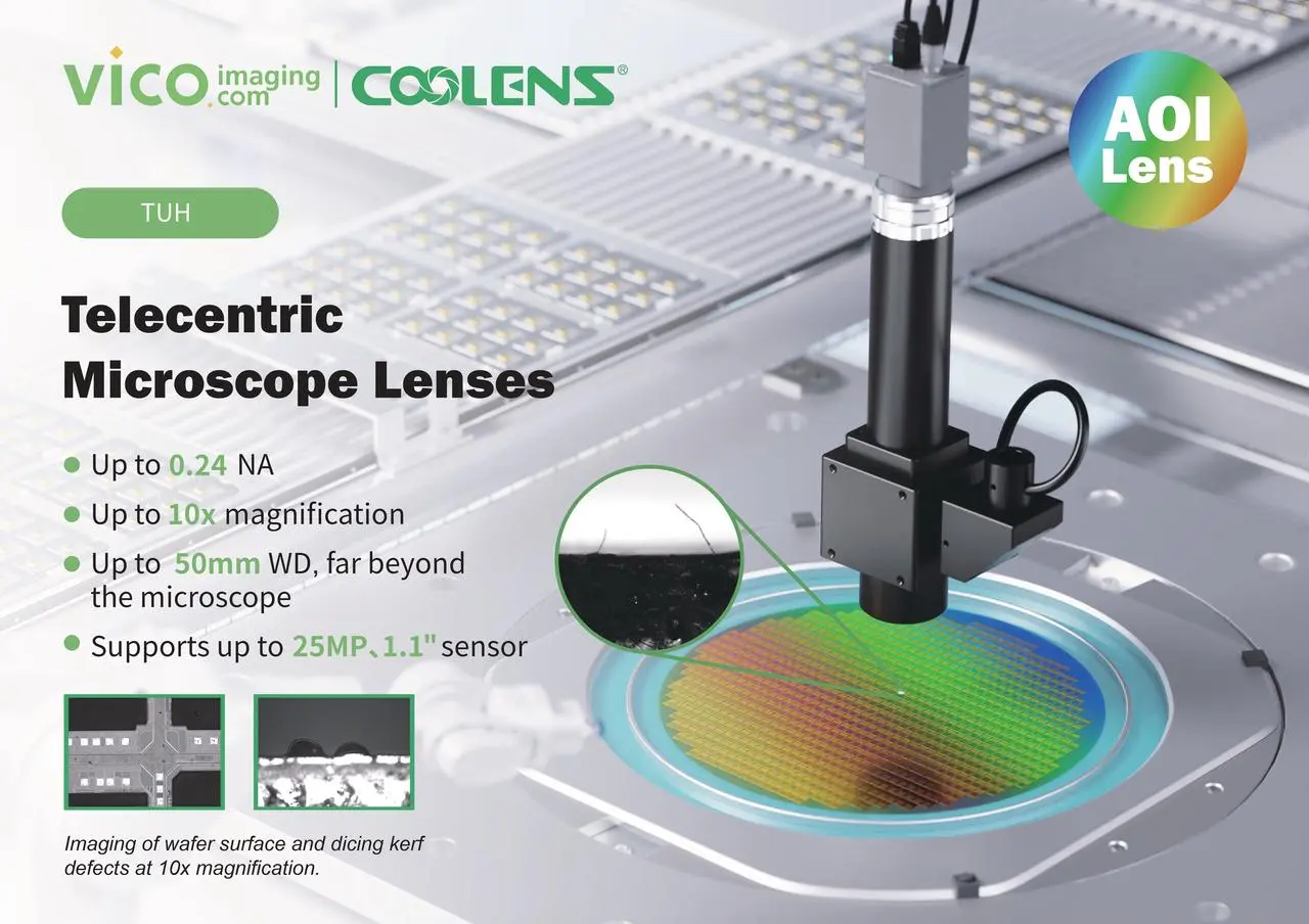
COOLENS® TUH Series for Wafer Dicing Inspection
Issues
- Limited operational space.
- Difficult illumination setup.
- Tiny defects.
Highlights of the TUH series
Using our TUH lens, up to 50mm WD provides you with greater flexibility for operation tasks. With built-in illumination, it frees extra lighting space. Our ultra-high resolution and magnification help you identify subtle chippings and burrs.
Key advantages:
- Up to 0.24 NA
- Up to 10x magnification
- Up to 50mm WD, far beyond the microscope
- Supports up to 25MP 1.1″ sensor
Solution
Configurations:
Lens: TUH100-50CT-111V2
Light: Built-in coaxial illumination, white light
Camera: 1.1” 25MP 2.5μm
Results
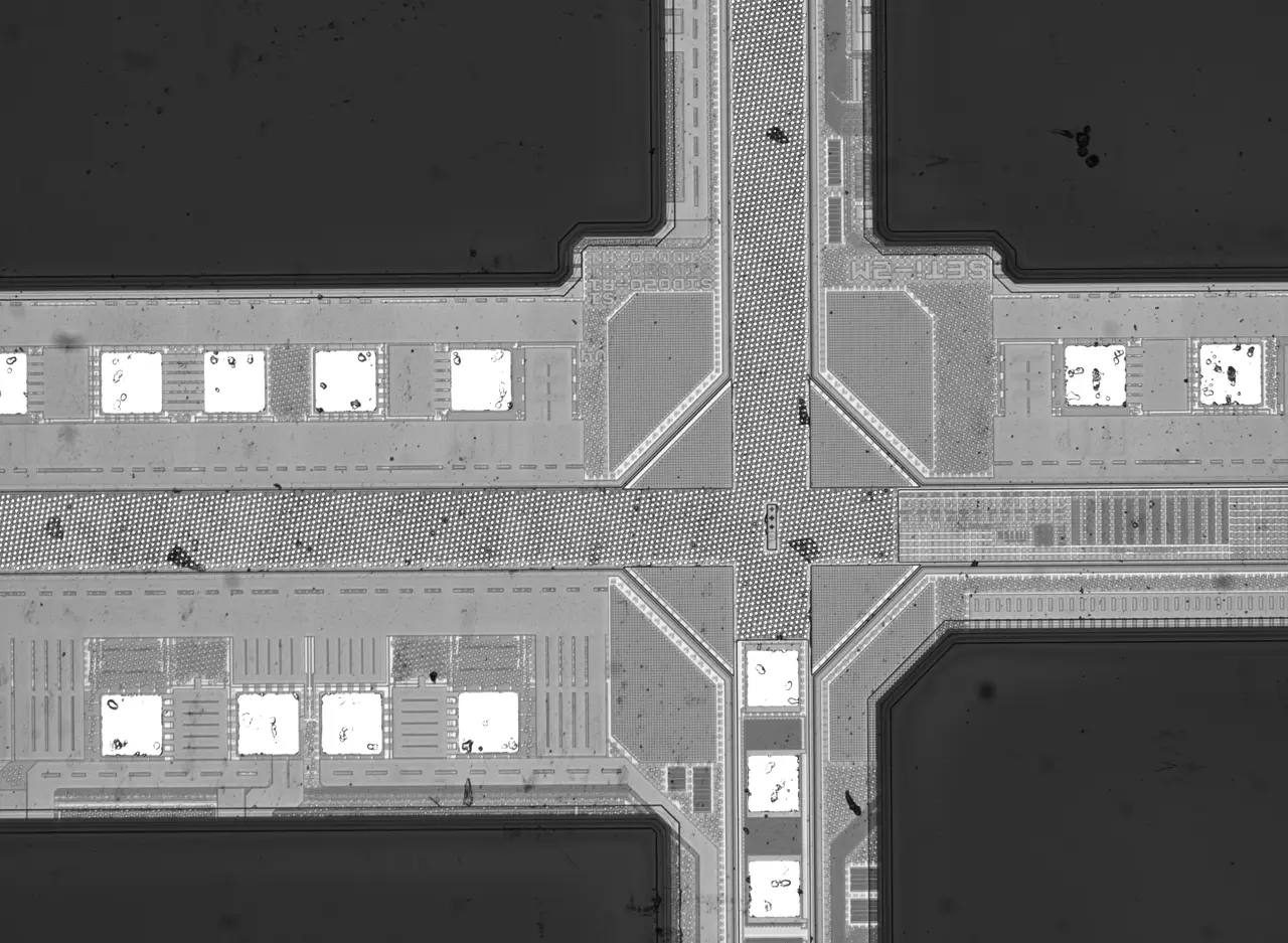
Defects are shown clearly in the two images. Burrs can be observed visually in the image ‘Wafer Dicing Kerf’. In the other picture, there are defects like scratches on the wafer surface.
Conclusion
As we summarize our sneak peek of VICO Imaging’s showcase at Japan ITE2024, we’re excited to invite you to experience our latest advancements firsthand. Please visit us at Booth No.2 to explore how our innovative products are driving progress in machine vision and shaping the future of industrial applications. We welcome you to schedule a detailed discussion and connect with us at sales@vicoimaging.com. For more information about this exposition, please click on our event page here.
