
The principles of imaging for industrial cameras
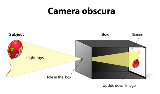 When a plate with a small hole is placed between the screen and the object, an inverted image of the object is formed on the screen. This phenomenon is called pinhole camera. As you move the middle panel back and forth, the size of the image changes. This reflects the fact that light travels in a straight line.
How camera works
Before the invention of the camera, people had already begun to use the principle of pinhole camera to create a variety of optical imaging devices, such devices known as the camera obscura.
In the first half of the 19th century, the camera industry was born out of the discovery of a method and medium for storing fixed optical images on the projection surface in the camera obscura, which is considered the ancestor of the camera. The lens is an intelligent pinhole, whose complex lens components can achieve different imaging distances (commonly known as focal length).
For a film camera, the reflected light from the scene is converged by the lens to form a latent image on the film, which is the result of the chemical reaction between the light and the emulsion on the film. The image is then developed and fixed.
The digital camera focuses the image on the imaging element CD/CMOS through the optical system and converts the photoelectric signal on each pixel into the digital signal through the A/D converter, then it is processed into a digital image by digital signal processor (DSP) and stored in a storage medium.
Image sensor
An image sensor or imager is a sensor that detects and transmits data used to form images. It does so by converting the variable attenuation of light waves (as they pass through or reflect off objects) into signals, which are tiny bursts of current that carry the information. The waves can be light or other electromagnetic radiation.
The two main types of electronic image sensors are the charge-coupled device (CCD) and the Complementary Metal Oxide Semiconductor (CMOS).
Read related post> Classification Of Cameras In Machine Vision Systems
Sensor size
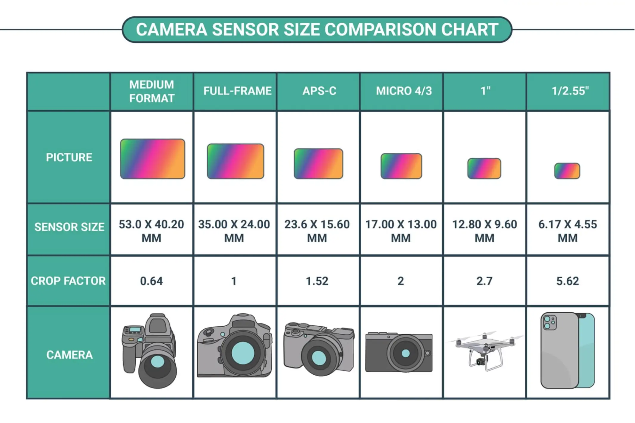 The region of validity of the camera sensor is crucial in determining the field of view (FOV) and the primary magnification (PMAG) of the system. For a fixed primary magnification (depending on the imaging lens), a larger sensor can provide a larger FOV. There are several standard area scanning sensor sizes. These standard terms can be traced back to the Vidicon vacuum tube used in television broadcast imagers, so it’s important to note that the actual size of the sensor will vary. However, most of these standards maintain a 4:3 (horizontal: vertical) aspect ratio.
One of the common problems in imaging applications is whether an imaging lens can support certain sensor sizes. If the sensor is too large for the lens design, then the resulting image will appear to fade with blur and degrade at the edges (light fading through the outer edge of the imaging lens). This is often called the tunnel effect because the edges of the FOV become dark. Smaller sensors will not have this problem.
CCD
CCD (Charge-Coupled Device) is a CCD image sensor. It is a semiconductor device that converts an optical image into a digital signal. The tiny light-sensitive material embedded in the CCD is called a pixel. The more pixels a piece of CCD contains, the more light-sensitive it is, and the higher the image’s resolution. CCD works like film, but it converts pixels into digital signals. CCD has many neatly arranged capacitors that sense light and turn images into digital signals. Each small capacitor, controlled by an external circuit, can transfer its charge to its neighbour.
CCD image sensor can directly convert an optical signal into an analogue current signal, the current signal is magnified and converted to an analog-digital signal to achieve image acquisition, storage, transmission, processing, and reproduction, CCD has the following characteristics:
- Compact and lightweight;
- Low power consumption, low work voltage, shock and vibration resistance, stable performance, and durability;
- High sensitivity, low noise, and wide dynamic imaging range;
- Fast response, self-scanning, low distortion, and no residual image;
- It is produced by large-scale integration technology with high pixel integration, accurate size, and low cost.
Read related post> How the CCD vision system determines the focal length of the required industrial lens
CMOS

CMOS (complementary Metal Oxide Semiconductor) is a kind of voltage-controlled amplifier, which is also the basic unit of CMOS digital integrated circuit. In the field of digital images, CMOS is invented as a kind of low-cost sensor. The common sensor in the market is CCD or CMOS.
The current situation is that many low-end digital cameras use low-cost CMOS chips, and the imaging quality is poor. Popular, advanced, and professional digital cameras use different levels of CCD.
CMOS manufacturing processes are used to make photoreceptors for digital imaging devices, which convert purely logical functions into electricity after receiving external light, then the image signal is converted into digital signal output by ADC on the chip. The characteristics of CMOS are as follows:
- Strong noise generated in the imaging process;
- High integration;
- Readout fast, and the address switch can be sampled randomly to gain higher speed.
CMOS has high integration, with short distances between components and circuits. This leads to serious interference, and noise has a great influence on image quality. The continuous development of CMOS circuit de-noising technology provides a solid foundation for the production of high-density and high-quality CMOS.
CCD V.S. CMOS

CCD and CMOS cameras differ mainly in five aspects:
- The way the information is read
The charge information stored in the CCD needs to be read after being transferred bit by bit under the control of the synchronous signal. The transfer and reading of the charge information output need to be coordinated with the clock control circuit and three sets of different power supplies, making the whole circuit complex. CMOS directly generates current (or voltage) signals after photoelectric conversion, making signal reading very simple.
- Speed
CCD needs to be controlled by a synchronous clock to output information one bit at a time, which is slow, while CMOS can take out electrical signals and process image information of each unit simultaneously when collecting optical signals, much faster than the CCD.
- Power supply and consumption
Most CCD devices require three power supplies and consume a lot of power, while CMOS devices use only one power supply, and it consumes only 1/10 ~ 1/8 as much power as CCD devices. CMOS has significant advantages in energy efficiency.
- Imaging quality
CCD technology, starting early on, isolates noise using a PN junction or a silicon dioxide (SiOz) isolation layer, giving it advantages over CMOS technology in terms of imaging quality. On the other hand, due to the high integration of CMOS, the proximity of optical sensors and circuits makes it susceptible to optical, electrical, and magnetic interference, leading to serious noise issues and affecting imaging quality over time.
However, in recent years, continuous advancements in CMOS circuit de-noising technology have created favourable conditions for producing high-density and high-quality CMOS image sensors.
- Internal structure
The CCD imaging points are arranged in an X-Y matrix, with each point consisting of a photodiode and an adjacent charge storage area controlled by the photodiode. The photodiode converts light (photons) into electric charge (electrons), and the number of electrons gathered is proportional to the intensity of the light.
When these charges are read, rows of data are moved to a buffer perpendicular to the direction of charge transfer. The charge information in each row is continuously read and then sensed by a charge/voltage converter and an amplifier. The resulting image has low noise and high performance.
However, the production of CCD requires clock signal and bias technology, making the whole structure complex and leading to increased power consumption and cost.
The electronics surrounding CMOS, such as digital logic circuits, clock drivers, and A/D converters, can all be integrated into the same process. The CMOS sensor is constructed like a memory, with each imaging point containing a photodiode, a charge/voltage conversion unit, a reset and select transistor, and an amplifier.
Besides, the entire sensor is covered by metal interconnectors (timing applications and reading signals) and vertically aligned output signal interconnectors that can easily read signals using X-Y addressing technology.
Read related post> The Difference Between CCD And CMOS
Conclusion
Image sensors are used in electronic imaging devices of both analog and digital types, which include digital cameras, camera modules, camera phones, optical mouse devices, medical imaging equipment, night vision equipment such as thermal imaging devices, radar, sonar, and others. As technology develops, electronic and digital imaging tends to replace chemical and analog imaging.
Since we have previously introduced CCD, CMOS, and the differences between them, when the inspected subject is in motion, either CCD or global exposure CMOS mode can be selected. However, currently high quality CMOS can cover the function of CCD, so CMOS is also a good choice.
