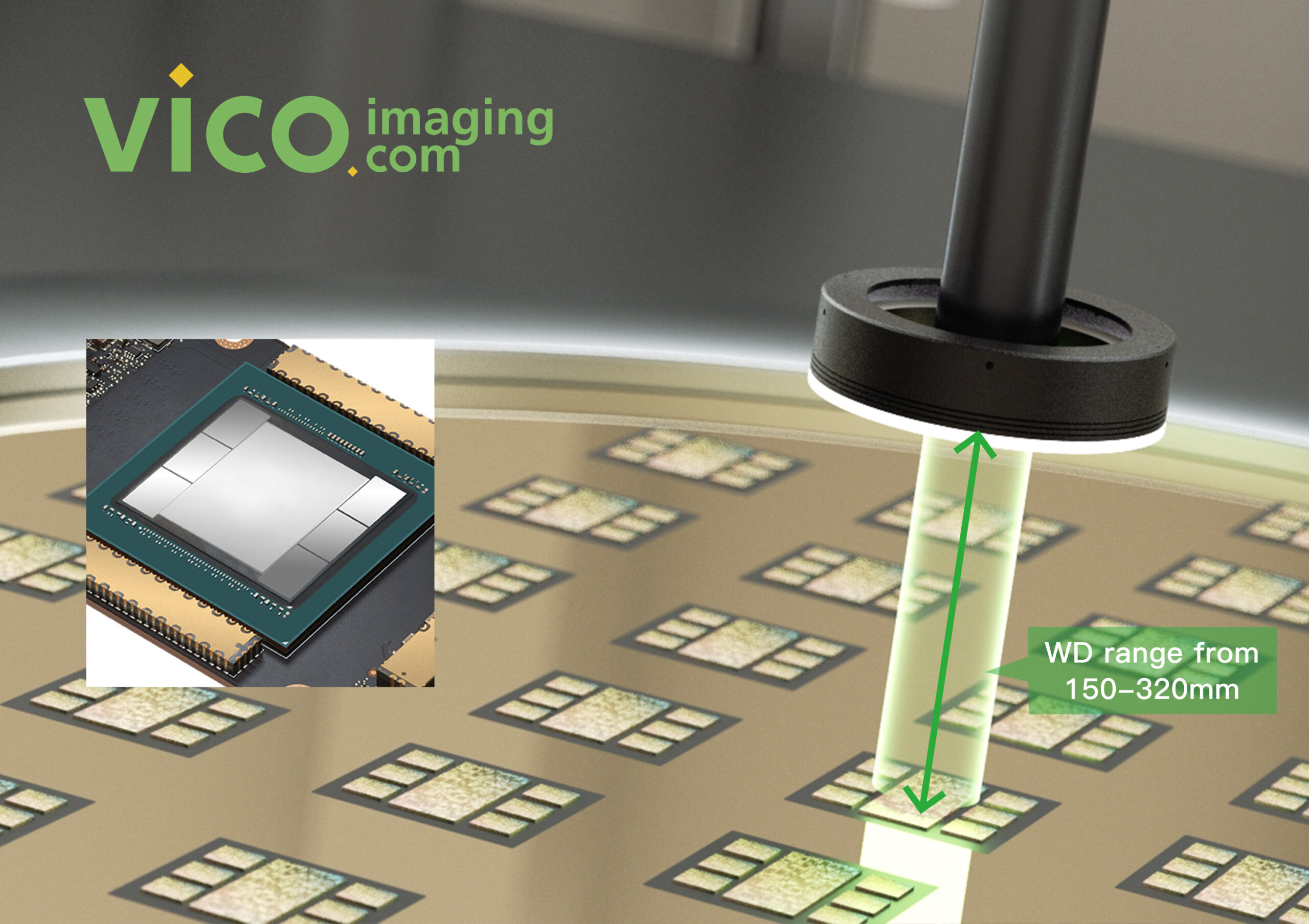
The new trend of 2.5D/3D semiconductor packaging technologies has issued a new challenge for inspection cameras – as the stacking process now requires the lens to accurately capture visual data not only on width/length but also on the 3rd dimension of height.
The 2.5D and 3D packaging is done by stacking IC dies on an interposer or even one another for multiple layers, greatly reducing footprints and size while increasing density and heat efficiency.
The traditional industrial lens used for IC packaging inspection now needs to keep up! Fret not! With the new WH04 Series and its long WD and large DOF, you can easily fit a robotics arm or other actuators while maintaining excellent imaging qualities on every stacking dies and their angles and positioning.
 |
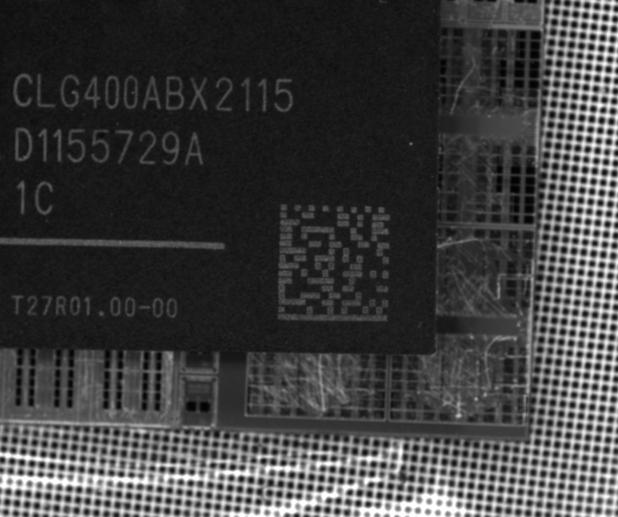 |
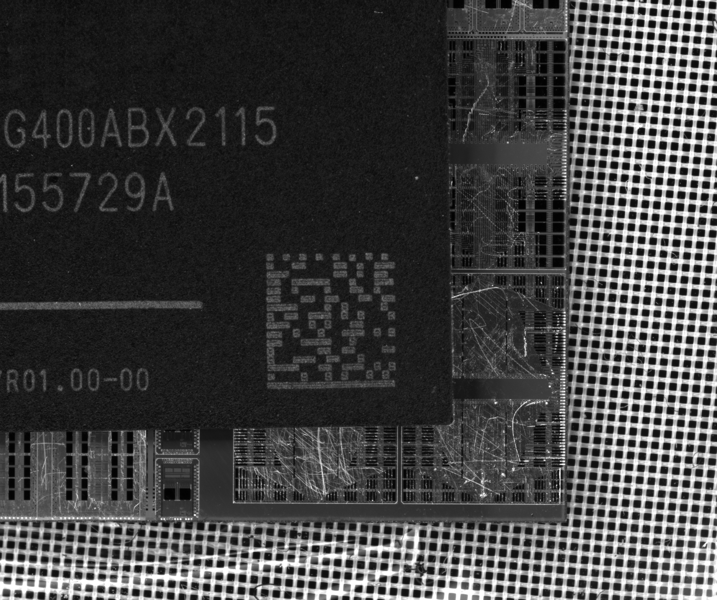
| COOLENS® WH04-320A-111 | one famous brand |
| (The total thickness from the upper surface to the lower surface of the measured object in the figures is 6mm.) | |
Main Features:
- Extra long WD: 150-320mm, allowing for more compact IC production solutions and saves tons of space.
- Larger DoF: Inspect through WH04 series lens and get every detail on multiple stackings.
- Magnification available from 0.3X to 0.7X .
- 1.1″ sensor supported.
As the designated lens for IC inspection by multiple industry leaders, the WH04 series is capable of meeting inspection needs for the most cutting-edge packaging trends, including CoWoS. Our in-house optics experts also provide extensive technical support including result image lab testing, providing total solutions and extensive after-sales consultation and adjusting. We have global offices covering countries and regions like South Korea, Germany and more.