About 2.5D/3D IC packaging
 2.5D/3D IC packaging is a revolutionary technology for the semiconductor industry, bringing significant power and performance benefits, promising to change the design constraints of processors, and providing a new way to overcome traditional die manufacturing limitations. As manufacturing processes improve and demand for high-performance computing grows, 2.5D/3D IC packaging technology plays a critical role in driving the future development of electronic devices. This technology not only improves space efficiency but also reduces power consumption and costs. However, it imposes stricter criteria on the inspection process, bringing greater challenges for traditional inspection.
In the era of AI, high computing power sets strict requirements for the transmission rate and information density for dies.
Engineers should not only ensure connection quality, but also meet the needs of reducing production costs, reducing power consumption, and designing for miniaturization in the packaging process. As a result, 2.5D/3D IC packaging technology has gradually evolved from the die bonding stage to the current 2.5D/3D packaging stage.
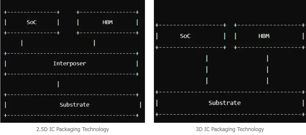
Here is a general picture of 2.5D and 3D packaging. It is to install two dies on the same interposer, then place the interposer on the PCB substrate, and then stack them together to form a complete die. This interposer allows the two components/dies to make an extremely dense information connection, thereby reducing signal transmission time and power consumption. This technique, which includes the interposer, is known as 2.5D IC packaging. In comparison, the method of removing the interposer and directly stacking each die together is 3D IC packaging.
For example, bumps in a microprocessor can be positioned vertically across many dies to reduce wiring distance, latency, and power consumption between blocks. Different new technologies can also be merged into 3D IC packaging, such as stacking DRAM on a CPU to lower power consumption and interface latency, without the need to integrate the technology into a single workflow.
The challenge
 Although 2.5D/3D packaging technology has numerous benefits, its application faces significant technical challenges, such as increased design complexity, thermal management issues, and difficulty in TSV fabrication and control.
In the meantime, the Automated Optical Inspection (AOI) encounters new obstacles while inspecting 2.5D/3D packaging. Compared to traditional packaging, 2.5D/3D packaging installs two chips on the same interposer, places the interposer on the PCB substrate, and then packages them together to form a full die. This approach stacks the chips, which may result in a height discrepancy.
Observing 2.5D/3D packaging from different angles, we will notice that the thickness and height of the stacked chips vary. Besides, the chip is very tiny, so the inspection during the post-packaging stage requires precise detection of tiny defects on the chip.
In general, to inspect defects in several layers with a single image, a large depth of field and high-resolution designs are required so that the image is clear enough to show damage and misalignments while still ensuring proper placement.
The role of our lenses in 2.5D/3D IC packaging
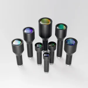
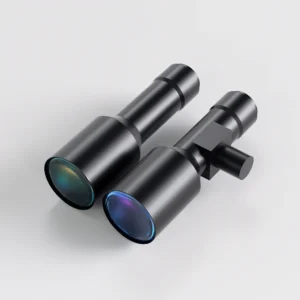
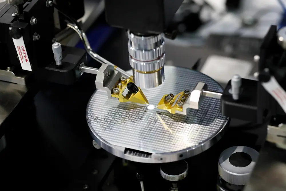
VICO Imaging is a game changer in the field of semiconductor inspection. Our lenses were designed specifically for the 2.5D/3D IC packaging process, and they play a crucial role in ensuring the quality and accuracy of chip assembly. Manufacturers’ vision inspection solution is an important part of the mid-inspection phase of the packaging process, focusing on detecting damages and misalignments as well as ensuring the correct placement of chip components.
The solution
Although imaging typically pursues high resolution, in the inspection stage after stacking, due to the layer difference/thickness, a lens with a large depth of field can capture features at different heights at the same time.
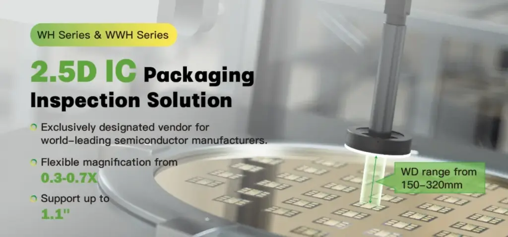
Our COOLENS® WH Series & WWH Series lenses have a large depth of field. This means that it can keep the image magnification consistent within a specific object distance range, thus allowing die features at different depths to be easily imaged. This is especially important for the inspection of multi-layer dies in the 2.5D/3D packaging industry, as dies at different levels may be located at different depths.
As a result, using these two series of lenses in 2.5D/3D packaging allows for the acquisition of a comprehensive image at once. At the same time, the image is clear, showing the flaws and skewness of the tiny dies. Overall, these two series are the ideal choices for 2.5D/3D packaging inspection.
Our lens inspection is mainly used in the post-packaging process. At this stage, we need to focus on the following aspects:
- Thickness inspection: Height and thickness inspection in 2.5D and 3D packaging is particularly important relative to traditional packaging.Spacing inspection: The spacing between wafers needs to be inspected to ensure uniformity and reliability of the stack.
- Spacing inspection: The spacing between wafers needs to be inspected to ensure uniformity and reliability of the stack.
- Alignment inspection: During the stacking process, it is critical to ensure precise alignment between the layers of chips. Misalignment can cause electrical connections to fail, affecting product performance.
- Defect inspection: Detects physical defects such as scratches, cracks, and foreign objects during the packaging process. These imperfections can affect the performance and service life of the chip.
In general, 2.5D/3D packaging technology uses silicon interposers or multiple-chip stacks, which require higher height and thickness. Therefore, precise inspection is essential to ensure the durability of packaging. At the same time, due to the need to detect height differences at multiple levels, the inspection equipment must have a large depth of field to accurately identify features at various levels.
It is essential to note that stacking is only one step in the packaging process. Our automated inspection technology is mainly used in the post-packaging process, namely to inspect the thickness, defects, and spacing of dies. At the same time, throughout the stacking process, it is crucial to ensure accurate alignment between chip layers. Misalignment may cause electrical connection failure, affecting product performance. By precise inspection, we can ensure the service life and performance of packaging, thereby improving the overall product quality.
The results and benefits
- Large depth of field
Since dies at different levels may be positioned at different depths, the large depth of field allows the characteristics of dies at different depths (whether they are skewed, damaged, or have tiny defects, etc.) to be fully and accurately captured at once. This reduces the number of shots, thereby saving time and increasing efficiency.
- Long working distance
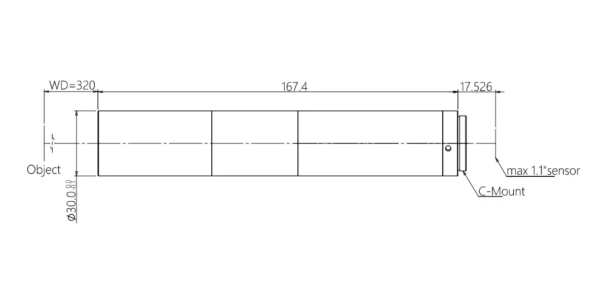
Adjustable magnification from 0.3X to 0.7X makes scenarios that require a long working distance possible. WH series lens, with up to 320mm working distance, allows for inspection not interfering with the production line, resulting in greater flexibility and reduced layout constraints. In doing so, the design of a long working distance saves system space and gets costs down.
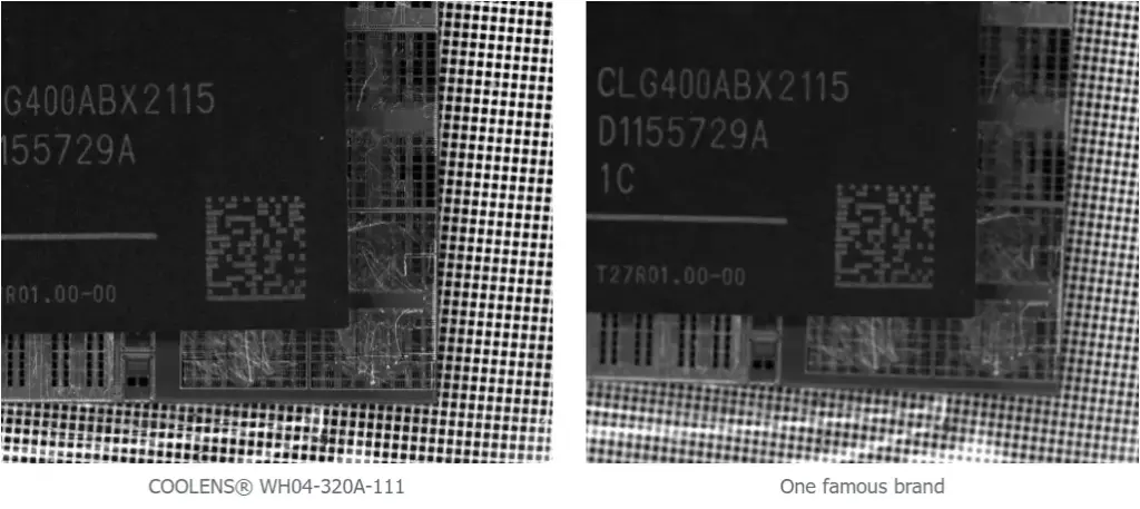
- Low distortion
The design principle of the telecentric lens makes its chief light parallel to the lens’s optical axis. This design effectively minimizes the image distortion caused by the change in distance between the lens and the object. This is crucial for 3D packaging inspection, which requires precise measurement and positioning.
- Multiple specification options
WH Series lens offers clients multiple choices so that they can choose lenses according to the specific requirements of their vision system.
Conclusion
Semiconductors have become a crucial technology, with applications in various industries including automobiles, data centers, smartphones, and high-performance computing, and will continue to grow in importance. The advanced technology of 2.5D/3D IC packaging has brought about a new era of innovation at both the die and system levels. The original production inspection solutions face greater challenges. To help customers deliver high-quality products, we are excited to launch the COOLENS® WH Series & WWH Series. These series lenses feature a large depth of field and high resolution for inspection in 2.5D/3D IC packaging. Semiconductor manufacturing always pursues perfection. Every component, no matter how minor, is critical to the final product. Therefore, advanced semiconductor production technology complements our lenses to bring unlimited possibilities for customers’ innovation. Contact us right now! Our experts can help you find the best lens for your needs.